

This is the third piece in a series exploring key semiconductor manufacturing equipment that China needs to indigenously produce high-bandwidth memory (HBM), perhaps the most important bottleneck in its efforts to make AI chips. The first piece was on advanced etching machines, while the second looked at the tools China requires for through-silicon via formation.
Chemical-mechanical planarization (CMP) is a crucial step in semiconductor manufacturing, required for producing advanced AI chips. My assessment is that China’s tools, primarily those from the leading Chinese firm Hwatsing, are good enough to produce indigenous HBM3, China’s near-term target. I would bet that this indigenization progress will continue, and that wafer polishing will not be a bottleneck for China’s AI chip ambitions.
At the end of May 2026, Huawei made a media splash with its new Tau Scaling Law, which it posited as the future of the semiconductor industry. Rather than scaling performance via transistor density, it proposes measuring performance in terms of time: how quickly information can flow through all the elements of the chip and the wider system. This is Huawei’s variant of the more-than-Moore trend that has been a key focus of the semiconductor industry. This focus on how chips can be cleverly assembled and interconnected to improve system performance is known as advanced packaging.
Huawei’s interest in advanced packaging also stems largely from the difficulties China faces in chip manufacturing. Due to export controls, especially those on extreme ultraviolet lithography machines, Chinese chip designers cannot effectively push their production below the 5 nm node. Western chip designers such as NVIDIA can push performance at both the manufacturing level (cramming more transistors onto chips) and the advanced packaging level (improving performance by how logic and memory chips fit together in a single package). Huawei cannot do the former, so has to go all in on the latter.
Jumping ahead of the global technological frontier is not easy, though. Huawei’s key approach is called LogicFolding, where a chip’s circuitry is split across two dies that are stacked on top of one another, increasing the density of the package without shrinking the transistors themselves. Huawei admits, however, that this ambitious technology will not be suitable for its AI chips until around 2030, and will only be used in its smaller mobile processors until then.1 Even so, advanced packaging will be one of the most important ways Huawei seeks to improve the performance of its AI chips over the medium term.
The current frontier of advanced packaging for AI chips centers on high-bandwidth memory. As explained in the previous pieces in the series, HBM is a critical component of AI performance, composed of layers of dynamic random-access memory (DRAM) dies connected via tens of thousands of tiny vertical wires called through-silicon vias (TSVs). Several types of machines are needed to connect all these DRAM dies into a single HBM stack and then integrate the rest of that stack onto the broader AI chip.
One of the required tools is chemical-mechanical planarization. CMP is among the more successful areas of Chinese indigenization. China’s leading firm producing CMP tools, Hwatsing (华海清科), has developed a portfolio of tools including ion implantation and cleaning, but its core product line is CMP machines, with over 1,000 units shipped and adopted in volume by several of China’s leading chip manufacturers, such as CXMT and YMTC. Crucially, CXMT has procured CMP tools from Hwatsing for HBM production.2
China also has a growing ecosystem beyond Hwatsing. At the end of 2025, AMEC, one of China’s largest equipment firms, moved to purchase Zhonggui (杭州众硅电子), Hwatsing’s most credible emerging competitor in CMP tools. This will give the relatively small start-up the full force of AMEC’s R&D platform and customer relationships to close the gap with Hwatsing.
CMP as a category is not among the semiconductor equipment items specified under US export controls. This means it falls under broader baseline restrictions, and has an easier time being exported to China, with the caveat that CMP is controlled for restricted end-users (those on the Entity List) and for restricted end-uses (advanced logic or DRAM production).3 Domestic producers thus have an advantage in selling to leading firms subject to either of these controls, such as YMTC or CXMT, but otherwise face continued competition from US and Japanese peers.
My view is that China very likely has sufficient domestic CMP capabilities to handle indigenous HBM3 production, a standard roughly two generations behind the current frontier, first produced by SK Hynix in 2022. The greater uncertainty is whether China’s future CMP machines can continue progressing and reach the more demanding levels needed for future hybrid bonding and more advanced HBM generations. I expect this to be a bright spot in China’s semiconductor efforts, given it has already likely reached the HBM3 level, and the overall emphasis in China’s ecosystem on advanced packaging and hybrid bonding as key methods for accelerating its memory capabilities.
In this post, I first explore the basics of CMP, how it works, and its role in HBM production. I then examine what makes CMP for advanced packaging difficult and how China’s capabilities stack up against their Western equivalents. I next dive into China’s CMP supply chain, exploring Hwatsing in depth, along with its two key competitors. I conclude with a summary of the outlook for China’s CMP industry and open questions about hybrid bonding.
Flat wafers are good wafers
CMP plays a simple but important role in semiconductor production, accounting for 6% of the hundreds of steps involved in wafer processing. After patterning with photolithography, etching away material, and depositing new materials, there is a need to tidy up. The silicon wafer, with these layers of new material on top, needs to be flattened so that a new layer can be formed. As the name suggests, CMP tools do this through a combination of abrasive chemicals and physical polishing. This sounds simple but is difficult in practice because it requires an incredibly high standard of planarization—creating an ultra-smooth, flat surface—while avoiding impurities, scratches, and other defects that can easily emerge when grinding away material.
CMP is needed for all the major elements of HBM production: producing the DRAM dies and base dies that were the subject of the first piece in the series, as well as the through-silicon vias explored in the second piece, and the advanced packaging stages that integrate HBM into the wider chip. Different stages are more or less difficult depending on the material being removed and how much needs to be removed. For example, removing large volumes of copper at high throughput with precision is trickier than removing a more even, thinner layer of dielectric material.
A CMP tool is split into CMP modules and cleaning modules.4 A diagram is below, but in simple terms, the wafer is placed inside a polishing head, which holds it in place and then rotates it over a specially designed pad covered in abrasive chemical slurries that strip away material. It is a chemical process because the materials in the slurry react with the materials in the wafer, softening or removing them. It is also a mechanical process because the wafer is physically pressed down onto the pad, so that particles on the wafer, softened by the chemicals, can be peeled away. The force is kept as low as possible to avoid damaging the structures on the wafer.
One analogy is rubbing rust off a piece of metal, where exposure to oxygen has produced an oxide variant that is more easily removed. This is how CMP works with materials like copper, just at a much faster and more controlled rate.
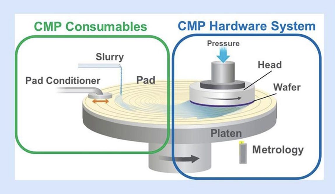
CMP has a reputation as a dirty process that generates large numbers of unwanted particles, hence the need for the cleaning modules. Rather than the pure vacuum chambers and sci-fi techniques of photolithography or etching, the wafer is sloshed around in chemicals and ground down. So the main risk of CMP is that it introduces impurities or defects into the wafer, which can severely reduce the yield of the process line—the share of chips that come out working. Small impurities from CMP can carry over to other process stages and tools, causing wafers to be defective and discarded.
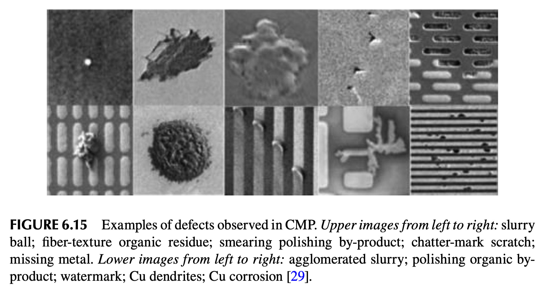
The best CMP tools introduce as few impurities or defects as possible and have robust integrated cleaning modules to remove any that do get introduced before they degrade the production line’s yield. CMP for advanced nodes just raises the necessary level of precision and cleanliness. Ever smoother surfaces are needed, at good throughput, and without even a speck of a particle.
CMP is not just about the tool, however; it also involves consumable inputs. The pad on which the wafer is polished needs to be replaced often, after just 400-800 wafers, depending on the material. A large DRAM fab will process more than 100,000 wafers a month, with CMP required at many stages, meaning thousands of replacement pads a month. The slurry needs to be tuned to the exact process requirements, ensuring the right chemical mix for the materials on the wafer. These consumables need to be highly consistent so that small changes in the chemical composition of the slurry, for example, don’t upset the CMP tool’s parameters.
Chinese firms have made some progress in pads and slurries, notably in gaining domestic market share, with slurry leader Anji (安集微电子) and pad maker Dinglong (鼎龙股份) both hitting number two in their categories, with shares of the Chinese market of 23% and 39% respectively in slurries and pads.5 This reflects extensive indigenization at mature nodes, though whether they have advanced-node capability is murkier, and I couldn’t establish a clear picture from their financials.
Through-silicon vias are demanding on CMP
Advanced packaging processes, such as carving through-silicon vias into DRAM wafers for HBM, can be especially challenging for CMP. They often involve thicker films that need to be ground down, longer polishing times, and tighter tolerances.6 Uneven DRAM dies in an HBM stack quickly cause issues: bonds fail to reach each other, or need greater bonding pressure, which can crack the die.
The previous piece in the series explored TSV formation up to the copper electroplating stage. This leaves the wafer with excess copper on top that needs to be removed to leave just the desired TSV:

Removing all this excess copper can be slow, and long CMP processes can cause variations in the wafer surface, as materials react slightly differently to the slurry chemistries or respond to inconsistencies in the pad. These tiny variations can build up over time and easily cause yield losses.
CMP tools can respond to these challenges by tailoring the chemistries, the pads, the pressure, or by introducing heat to accelerate the copper removal.7 Getting these recipes correct, as well as having good measurement tools integrated into the machine to track any emerging variations, is vital. The best CMP tool is one that makes this learning and iteration process as easy as possible for the chip manufacturer.
Demands on CMP are likely to rise further due to the move towards hybrid bonding. Currently, the TSVs in all the DRAM dies are stacked using solder microbumps. These are little blobs of metal that connect the TSVs, and are usually formed using a process called thermo-compression bonding.8 Microbumps do the job but are undesirable. They increase the stack height, reducing the number of DRAM dies that can fit. They are also worse than hybrid bonding in the density of interconnections they enable and in their power efficiency.
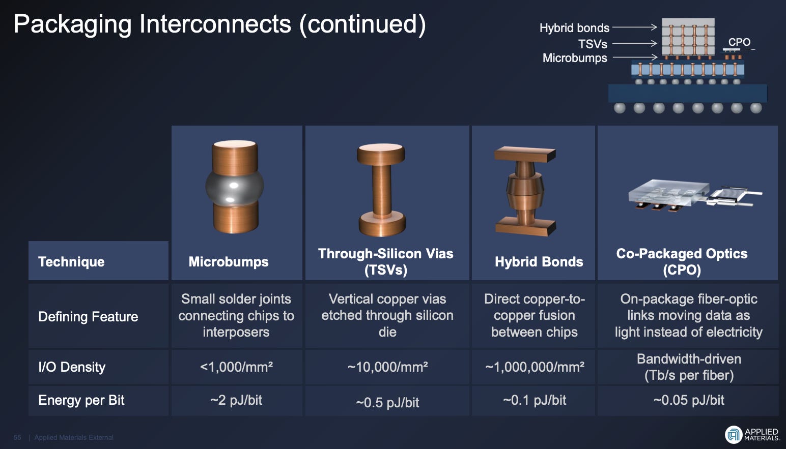
Hybrid bonding disposes of the solder bumps and directly fuses the two dies together, connecting the copper TSVs to one another and to the surrounding dielectric materials. This lowers the height of the HBM stack, allowing more layers of DRAM. It is also more energy efficient and enables better interconnection.
Hybrid bonding was originally intended for the current HBM4 generation, but was dropped in favor of keeping the solder microbumps. It remains the next major leap on HBM product roadmaps, but one that none of Samsung, SK Hynix, or Micron has yet taken.
Hybrid bonding leaves little room for error. The copper bond pads for the TSVs need near-perfect alignment, and there can be almost no impurities between them; otherwise, you will disturb the bond. CMP is critical because the two dies need to be as flat and level as possible so they can be properly bonded. While solder bumps can get away with accuracy at the micron level, hybrid bonding needs surface polishing down to 0.5 nanometer precision, orders of magnitude finer.
A further difficulty is that DRAM dies for HBM are thinned to tens of microns, thinner than a human hair. To squeeze in as much DRAM as possible, you want these very thin dies. But thin dies bend and bow much more easily, the opposite of the absolute flatness required for hybrid bonding.
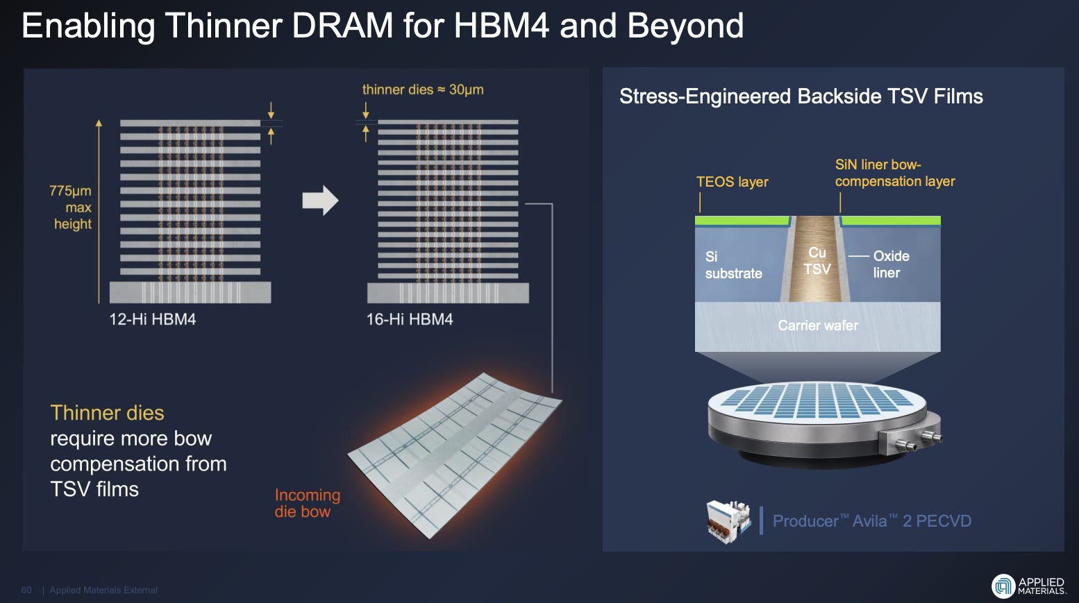
These hybrid bonding challenges are the focus of the leading Western tool makers. For example, Applied Materials released its Opta Quad CMP machine in June 2026, designed to address these advanced packaging and hybrid bonding issues through real-time pad temperature control and integrated measurement systems, enabling more precise wafer shaping.
Chinese CMP firms almost certainly still have work to do to raise the yields their products can achieve on older HBM3 and HBM3E. But the real prize would be to accelerate towards hybrid bonding and leapfrog Western companies. Given the manufacturing bottlenecks Chinese memory firms face in producing DRAM as capable as leading Western manufacturers’, this advanced packaging approach is their best bet to build a more competitive HBM product.
Hwatsing leads China’s CMP push
Hwatsing was founded in 2013 as a spin-out from Tsinghua University. The Laboratory of Tribology9 at Tsinghua had been researching CMP since 2000, and from 2008 took on one of the state-sponsored research projects under the 02 Special Project.10 The 02 Special Project was China’s key semiconductor industrial policy from 2006 through to the late 2010s and sought to indigenize elements of the global supply chain.
This research effort led to Hwatsing’s formation; it received 30 patents from Tsinghua as IP equity and licensed another 70. Hwatsing shipped its first commercial CMP tool in 2015, and continued development with state support.

Real mass production began in 2018. Revenue took off in the early 2020s as Hwatsing broke into procurement for major domestic expansion efforts, first at YMTC, which alone accounted for 66% of Hwatsing’s total revenue in 2021.11 In 2022, Hwatsing completed an initial public offering (IPO) on the Shanghai Stock Exchange and has since seen rapid growth. It shipped its 1,000th CMP tool in April 2026, possibly bringing it to 15-20% of Applied Materials’ install base.12 Hwatsing has not exported from China in any meaningful quantity, though its stated plan for 2026 expressed an interest in expanding into Southeast Asia.13
While Hwatsing has attempted to expand beyond being a CMP specialist to a wider platform that includes ion implantation and cleaning tools, it remains far smaller than peers such as Applied Materials, which had $28 billion in revenue last year across its broad portfolio. Applied Materials does not break down its revenue by tool segment, but it almost certainly remains significantly larger than Hwatsing in CMP, and its greater scale allows for higher R&D spending and cross-learning between its platforms.
Hwatsing’s 2022 IPO prospectus includes a helpfully detailed assessment of the technological gap it faced relative to its US and Japanese peers in CMP, Applied Materials, and Ebara. Hwatsing assessed it had “achieved process-technology levels of 14 nm (logic chips), 128 layers (3D NAND), and 1x/1y nm (DRAM) respectively”,14 compared to Applied Materials and Ebara at the 5 nm node—with the caveat that Hwatsing’s 14 nm was “under verification” and it had only 28 nm in volume production as of 2022.15
This establishes a clear baseline of how Hwatsing compared to Western tools in 2022:
Assessing Hwatsing’s position in 2026 is trickier: its recent filings are less descriptive, claiming only a qualitative “advanced logic” or “advanced memory”. One approach is to gauge the gap based on the most advanced nodes of Hwatsing’s customers. Doing so assumes that Hwatsing is shipping tools to the most advanced lines, which is somewhat unlikely, but could be the case with recent capacity expansion projects. Hwatsing’s tools could instead be better than what its customers’ most advanced nodes would require, though I would consider this even less likely given the relative immaturity of its tools. Even with these caveats, it provides at least some signal of what Hwatsing’s verified capabilities could be.
The picture is not particularly rosy for Hwatsing. While the gap has shrunk in NAND, it has grown in DRAM. The main limitation here, and one that Hwatsing flags in its own risk disclosures, is that its customers are held back from progressing to more advanced nodes. Due to export controls on advanced photolithography, etch, and deposition tools, firms such as SMIC, CXMT, and YMTC cannot progress towards the global frontier at the pace they otherwise would.
This makes it harder for Hwatsing to improve its CMP tools. The risk disclosure in Hwatsing’s 2025 annual report reads: “Compared with international leading competitors such as Applied Materials, the company’s technology and equipment lack opportunities for validation and application in more advanced IC mass-production lines; there is a gap in the technical level of advanced-process applications.”16 There is no domestic 2 nm logic or 1c DRAM node for Hwatsing to test its capabilities against and build up a stock of performance data from.
Hwatsing can push its own R&D, but its tools operate within an ecosystem of materials suppliers and chip manufacturers necessary to develop the tool and the broader process step. Absent a frontier node, it is difficult for Hwatsing to align with domestic producers of CMP pads, slurries, or tool sub-components to push towards the criteria for leading-edge production. For example, one of the core challenges of frontier CMP is reducing impurity rates, but these rates arise from a complex interaction among the tool, pads, and slurries, as well as the process recipe and stage being run. This is a many-sided challenge that Hwatsing cannot solve alone.
Hwatsing’s tools are likely good enough for current indigenous HBM production
The clearest signal that Hwatsing’s tools are good enough for domestic HBM comes directly from Hwatsing in its most recent annual report: “The company’s portion of advanced-node CMP equipment has entered the HBM lines of head memory manufacturers as baseline equipment.”17 The head memory manufacturer here is almost certainly CXMT. Direct sales into CXMT’s HBM lines are a very strong indicator that Hwatsing’s CMP tools can handle some production steps for CXMT’s G4/1z DRAM (which is now becoming its majority node). This does not tell us exactly what the tools are being used for in the line, whether that means trickier bulk copper removal steps of TSV formation or simpler polishing steps earlier in the process.
Ideally, there would be public information on exactly what Hwatsing’s tools were being used for, and the delta in yield versus Applied Materials and Ebara. Unfortunately, there is none, so the proxy that Hwatsing has at least sold into the relevant line is the strongest signal available.
One complication for China’s HBM efforts is that CXMT does not vertically integrate the entire process, unlike SK Hynix, Samsung, and Micron. Instead, later stages are contracted out to Chinese outsourced semiconductor assembly and test (OSAT) firms. These OSATs, such as Tongfu or JCET, traditionally handled simple late-stage packaging steps, but have become increasingly capable in the advanced packaging required for products like HBM. Hwatsing also claims that it “serves as benchmark equipment on advanced packaging production lines for HBM, 3D stacking, etc.”,18 suggesting it supplies these OSAT players.
The OSATs, though, need not only CMP tools but also thinning and edge-polishing tools. For one thing, these are not ultra-complex platforms of plasma and chemicals but rather the kinds of physical grinding and cutting tools you would expect, albeit dialed up to extreme precision and designed not to overstress or fracture the delicate die. Hwatsing introduced its first thinning tools in 2023, after taking on a national industrial policy project to do so in 2020.19 Its most recent tool in this category was a platform designed for advanced memory thinning, introduced in April 2026.
The real contrast between the CMP and thinning platforms is in their relative sales volumes. While Hwatsing has reported more than 20 cumulative units and more than 200,000 wafers processed for its oldest thinning machine as of December 2025, it hit over 1,000 CMP units sold in early 2026.20 For context, Applied Materials likely has an install base ~5x as large.21
As of early 2025, Hwatsing’s assessment of its position was:
Although the company’s CMP equipment has captured a relatively high market share domestically, the high-precision thinning equipment and wafer dicing equipment needed by domestic IC manufacturers remain heavily dependent on imports, which affects supply chain safety. Overseas wafer ultra-precision thinning and dicing started earlier; overseas thinning and dicing equipment suppliers represented by Japan’s DISCO have advanced technology and basically monopolize the global market.22
Hwatsing’s global market share in CMP jumped to 10% in 2023 and fell slightly to 9% in 2024; there is no data yet for 2025. Unfortunately, I haven’t found data on thinning tools, though the chart below shows its Japanese competitor DISCO’s China revenue, where no serious Hwatsing incursion is visible.
While Hwatsing has been growing rapidly, it remains smaller than its American and Japanese competitors; Applied Materials is almost 24x bigger by market cap.23 Hwatsing’s market share in CMP is likely to grow as Chinese firms increasingly purchase indigenous tools due to export controls. This will help it build scale over time, especially as it moves into other product verticals such as ion implantation.
The chart below shows Hwatsing’s revenue versus the total China-based revenue of Applied Materials, Ebara, and DISCO. The comparison is unfair in that all three comparators include revenue lines beyond CMP, but it is indicative of Hwatsing’s still-relatively small market position and the potential growth available to it. Growth will be needed to sustain the R&D intensity required to catch up to major global platform players such as Applied Materials.
The picture from Hwatsing’s financials is of a maturing core CMP business, and a younger, thinning product line that is likely seeing initial adoption and testing but is not yet a volume substitute for foreign tools in the way that its CMP line increasingly is.
Another way to assess Hwatsing’s capabilities is to look at its R&D goals. It plans to raise around $300 million in private financing for a project on “High-End Semiconductor Equipment R&D”.24 Two planks of this are R&D for its next-generation CMP platforms aiming to overcome “bottlenecks in equipment detection, precise control, advanced cleaning, and endpoint detection”,25 as well as expanding its thinning portfolio and working to “optimize mechanical structure & control algorithms”.26 It still has a long way to go to catch up with the market leaders’ technical capabilities.
My best assessment is that Hwatsing’s CMP tools are good enough for CXMT’s HBM production, handling 1z-node DRAM and the TSV formation stages that CXMT performs to produce TSV dies. They can produce working dies at a reasonable yield, even if there is still a minor yield disadvantage versus US or Japanese tools. Its CMP tools are also likely capable of the advanced packaging CMP stages required for TSV reveal and bonding of TSV dies into an HBM stack, which are undertaken by OSATs.
I am far less confident its thinning tools can handle the required advanced packaging stages; these are likely still in early testing and adoption, with potentially unviable yields for now. Since I expect Hwatsing to be rapidly moving up the learning curve given its now fairly extensive install base, including in China’s most advanced process lines, I don’t foresee CMP being a lasting bottleneck to China’s HBM production, with the remaining challenges perhaps solved in just a few years’ time.
AMEC has bought its way into being the key CMP challenger
Hwatsing is the clear leader in domestically produced CMP tools, claiming a market share of more than 90%,27 but it does have two significant domestic competitors. Both share roots in China’s more traditional state industrial complex via the China Electronics Technology Group Corporation (CETC). CETC was formed in 2002 as an amalgamation of older state electronics research institutes and is one of China’s largest defense industrial conglomerates.28
One of those research institutes, number 45, hosted CMP research. In 2015, Gu Haiyang (顾海洋) returned to China after 13 years at Applied Materials and became the general manager of CMP efforts at CETC-45. In 2018, he left CETC to found a new firm, Zhonggui.
After Gu’s departure, CETC-45 spun up its own commercialization vehicle in Jingyi Jingwei (晶亦精微科技) in 2019. Jingyi has had the most success in CMP tools for 8-inch wafers—the smaller wafer size used for mature (older-generation) nodes, whereas advanced production runs on 12-inch wafers. SMIC was one of its earliest customers, having already purchased the first 8-inch tools developed within CETC.
Jingyi attempted to IPO in 2023-24 on the Shanghai stock market but ultimately terminated its listing amid concerns about customer concentration (SMIC accounted for half of its total revenue in 2022) and legal disputes with Zhonggui during the review. Its own technical assessment in its IPO documentation was that its tools were capable of 28 nm and above, substantially behind Hwatsing.29 Since the collapse of its IPO in mid-2024, Jingyi has gone fairly quiet.
Of the two, the big winner, and Hwatsing’s most significant emerging competitor, has been Zhonggui. In December 2024, Zhonggui introduced its tools to a major customer—anonymized as “Group A” in the filings but quite likely CXMT30—and received a first round of investment from AMEC based on that achievement. It then saw follow-on orders in September 2025 and a further AMEC investment; in December, AMEC moved to acquire full control.31
Zhonggui remains far smaller than Hwatsing in revenue—$34 million in 2025 versus $650 million32—but claims that “Overall, compared with Hwatsing’s equivalent equipment, the Target Company’s 12-inch CMP equipment shows no significant differences in key performance indicators.”33 Zhonggui lists its tools as having “achieved industrialized application” at 1x/1y DRAM and HBM.34 These marketing claims are likely somewhat overstated, as parity with Hwatsing is not backed by actual customer wins or revenue.
Zhonggui’s integration into AMEC secures it a strong financing and R&D outlook, and if its major “Group A” customer is CXMT, that does position it as Hwatsing’s key competitor for HBM-relevant processes. With that backing, it could close the gap with Hwatsing fairly quickly. This head-to-head competition between Hwatsing and AMEC-Zhonggui is precisely what Beijing’s policymakers want to see.
CMP is unlikely to be a bottleneck to China’s HBM and hybrid bonding ambitions
CMP tools are unlikely to be a bottleneck to China scaling up its indigenous production of HBM3. For the required DRAM and advanced packaging steps, Hwatsing and, in a couple of years, AMEC-Zhonggui will have capable tools. The core bottleneck for domestic HBM3 production will remain in other areas, primarily photolithography.
China does not, however, want to be stuck at HBM3, but will be looking to push towards HBM3E and the current-generation HBM4. Lacking access to extreme ultraviolet lithography tools, China will need to rely more on advanced packaging techniques as it has less headroom in advancing DRAM nodes.35 Since their DRAM dies won’t significantly improve, Chinese firms will have to catch up on performance by cramming more of them into a single HBM stack than SK Hynix or Micron do.
Hybrid bonding is how this would be accomplished, and the best hope for Chinese memory firms to leapfrog and close the performance gap. This is likely already occurring, with the most important move coming from YMTC, China’s NAND giant, which has successfully adopted hybrid bonding techniques in NAND. It is now looking to enter the DRAM and HBM markets. It is reportedly cooperating with CXMT on HBM, where CXMT’s DRAM capabilities and YMTC’s hybrid bonding know-how seem a strong match. Huawei’s roadmap also explicitly integrates hybrid bonding for its Ascend GPUs around 2030, starting with the Ascend 990, for which it aims to use its LogicFolding design.
Hybrid bonding requires advances not in photolithography, where Chinese firms have struggled, but in advanced packaging, where China is already relatively strong. CMP would be one important piece of this. Success with hybrid bonding demands frontier performance in reducing impurities and far more precise control and measurement during CMP; it requires “dishing” to nanometer precision, meaning that the copper in the TSVs must be slightly recessed so that, when heated, it expands and forms a bond with its paired die. Current TSV formation requires only micron-level precision, orders of magnitude too coarse for hybrid bonding.
Hwatsing still undoubtedly lags Applied Materials in hybrid bonding capabilities, with its filings giving no indication that hybrid bonding specifically is an R&D focus. But what hybrid bonding demands generally overlaps with what Hwatsing needs to close the gap with Applied Materials: better in-line measurement, lower impurity rates, and higher throughput. This does not rule out Hwatsing advancing on this front.
I expect to explore bonding tools more in future work, but my take for now is that Chinese CMP makers are almost certainly not ready for hybrid bonding flows; my more tentative view is that by the time CXMT and YMTC seriously attempt hybrid bonding for HBM, perhaps in 2027 or 2028, they may be.
I wouldn’t expect CMP development to hold back China’s adoption of hybrid bonding at scale; the difficulty will more likely lie elsewhere in the process flow. Lack of access to extreme ultraviolet lithography continues to slow node development and harm yield; hybrid bonding tools themselves take extensive development; or perhaps China lacks the advanced metrology tools to make hybrid bonding work. China will need to pull all these pieces together to deliver hybrid bonding at a commercially viable cost, and so use it to expand its AI chip capabilities.
Huawei aims to integrate LogicFolding with the Ascend 990, scheduled for “around 2030”; see the full Huawei Tau Scaling paper.
See Hwatsing’s 2025 annual report, which claims its tools have entered the lines of a head memory manufacturer as baseline equipment, or see SemiAnalysis’ recent piece on CXMT.
In export control jargon, CMP does not fall under stricter advanced equipment rules such as 3B001, 3B993, or 3B994; instead, the most relevant provision is 3B991.b.1.k, which has a surface roughness element that would capture CMP tools, but then has a carve-out for “single-side lapping and polishing equipment for wafer surface finishing” that likely excludes front-side wafer CMP tools, with the focus on backside wafer thinning tools. As far as I can tell, they are not covered under Japanese controls so any controls would apply only if Ebara tools have sufficient US-origin technology to fall under the EAR.
See Planarization for Advanced Packaging and Hybrid Bonding for a good technical run-through of how CMP works.
See Dinglong’s HKEX listing application for these market share estimates by Frost & Sullivan.
See Applied Materials Advanced Packaging Master Class for how advanced packaging causes challenges for CMP.
See Planarization for Advanced Packaging and Hybrid Bonding and its section on copper removal CMP.
Samsung and Micron both use thermo-compression bonding, specifically thermo-compression bonding with a non-conductive film. This stacks each die one by one, using heat and pressure to bond the solder bumps, as well as soften the film, which flows into the gaps and then cures into a solid filler, effectively gluing the dies together. SK Hynix uses a different process called mass reflow molded underfill, which instead stacks all the dies together first, with all the solder joints formed collectively in a reflow oven, and then a liquid epoxy molding compound is injected to fill in the gaps.
For all those who, like me, need a reminder on tribology, it is the science of interacting surfaces in relative motion.
This detail on the company’s background comes from Hwatsing’s 2022 IPO prospectus.
Again see Hwatsing’s 2022 IPO prospectus and its section on customer concentration risks.
See one of the footnotes below for an estimate of Applied Materials’ install base at likely ~5,000 and potentially up to ~7,000.
See Hwatsing’s 2025 annual report, which gives a breakdown of non-mainland revenue, only 0.9% of its total, and even that is largely sales to foreign-owned fabs in China. The 2026 plan lists the Southeast Asia ambition as part of “deep cultivation in China, expand globally” (深耕国内、拓展全球).
From Hwatsing’s 2022 IPO prospectus, translated by Claude Fable 5, original Chinese: 其在逻辑芯片制造、3D NAND制造、DRAM制造等领域的工艺技术水平已分别突破至14nm、128层、1X/1Ynm,均为当前国内大生产线的最高水平.
From Hwatsing’s 2022 IPO prospectus risk disclosures, “The CMP equipment of Applied Materials and Ebara has reached the 5nm process-node level, whereas the company’s equipment is mainly used on 28nm-and-above production lines, with the 14nm process still under verification”, translated by Claude Fable 5, original Chinese: 美国应用材料和日本荏原所生产的CMP设备均已达到5nm制程工艺水平,公司CMP设备则主要应用于28nm及以上制程生产线,14nm制程工艺仍在验证中.
From Hwatsing’s 2025 annual report, translated by Claude Fable 5, original Chinese: 与国际领先的竞争对手美国应用材料等公司相比,公司的技术和装备缺乏在更先进的集成电路大生产线中验证和应用的机会,在先进工艺应用的技术水平上存在一定差距.
From Hwatsing’s 2025 annual report, translated by Claude Fable 5, original Chinese: 公司部分先进制程CMP装备进入头部存储厂商HBM产线作为基线设备.
From Hwatsing’s 2025 annual report, translated by Claude Fable 5, original Chinese: 报告期内,公司新签CMP装备订单中先进制程的订单已实现较大占比,公司高端系列CMP装备在国内多家头部客户实现先进制程节点工艺验证,并在HBM、三维堆叠等先进封装工艺产线上作为基准设备.
See Hwatsing’s 2023 annual report for this context: the first pre-production thinning tools were with customers by 2021, but commercial launch was only in 2023.
See Hwatsing’s 2025 annual report for both stats.
Applied Materials hasn’t disclosed a unit figure since 2011, when it claimed 3,000 tools at customer sites. These tools are long-lived and go through sequential upgrade cycles rather than being overhauled and replaced. Firms exist to maintain decades old Applied Materials CMP platforms. If the pace of sales (3,000 between the late 1990s and 2011) is similar for 2011-2026, that gets you towards 6,000-7,000 tools. Assuming some loss of older generations of tools, that discounts you towards ~5,000, 5x Hwatsing’s install base, but this estimate is quite uncertain.
From Hwatsing’s 2024 annual report, in the industry discussion section, translated by Claude Fable 5, the original Chinese: 虽然公司CMP装备已在国内取得较高市场占有率,但国内IC制造厂所需的高精密减薄装备和晶圆划切装备仍严重依赖进口,这将影响到供应链安全。国外晶圆超精密减薄和划切加工起步较早,以日本DISCO公司为代表的海外减薄和划切装备供应商具备先进技术,基本垄断全球市场.
These have been bouncing around, as of writing August 7th, Hwatsing’s market cap is RMB 120 billion (about $18 billion), while Applied Materials’ is $426 billion. 426 ÷ 18 is 23.7.
See Hwatsing’s notification of its Private Placement Plan.
From Hwatsing’s Private Placement Plan, translated by Claude Fable 5, original Chinese: 攻克设备检测、精准控制、先进清洗及终点检测等技术瓶颈,形成成熟稳定的配套工艺方案,开展抛光压力精准调控、超净清洗工艺优化、终点检测算法迭代等深度研究……并根据市场需求推出应用于先进逻辑、先进存储等高端制造工艺的新型号设备.
From Hwatsing’s Private Placement Plan, translated by Claude Fable 5, original Chinese: 在减薄领域……一是对现有减薄装备进行迭代,优化机械结构与控制算法;二是拓展高性能减薄装备新品类,攻关新型减薄工艺与适配技术……形成覆盖多领域的减薄装备产品矩阵.
From Hwatsing’s 2025 annual report, translated by Claude Fable 5, original Chinese: 占据国产CMP装备销售90%以上份额.
See CSET’s piece on “Pulling Back the Curtain on China’s Military-Civil Fusion” for more detail on CETC.
See Jingyi Jingwei’s SSE IPO inquiry reply, translated by Claude Fable 5, original Chinese: 发行人12英寸CMP设备尚未实现销售,在28nm制程国际主流集成电路产线完成工艺验证、尚未完成长期稳定性测试,已签订7个销售订单,制程工艺落后于国内外竞争对手.
The customer is specifically a group, with fabs owned by subsidiary firms, meaning it has to be a fairly large multi-fab player. The capabilities listed in Zhonggui’s April 2026 filing give 3D NAND as “in product design demonstration”, so YMTC can be safely ruled out. Zhonggui had already sold tools into SMIC prior to 2024, so it too can be ruled out. The other likely candidates are DRAM maker Fujian Jinhua or fabs within Huawei’s network, such as SwaySure. These are possible, but CXMT appears a cleaner fit, especially as it would also justify Zhonggui’s claim of having entered HBM product lines.
Zhonggui’s 2025 revenue is from its FY2024-25 Audit Report and was RMB 244.1 million (roughly $34 million at 2025 average rates). Hwatsing’s revenue is from its 2025 annual report, and was roughly $650 million using annual average exchange rates.
The full quote from the AMEC–Zhonggui Restructuring Report from April 2026 with cited KPIs: “Overall, compared with Hwatsing’s equivalent equipment, the Target Company’s 12-inch CMP equipment shows no significant differences in key performance indicators including stable tool uptime ratio, wafer breakage rate, removal rate, wafer-to-wafer non-uniformity, within-wafer non-uniformity, post-polish/clean defect control, and surface roughness—both can achieve 14nm (currently in verification) and above process technology.” Translated by Claude Fable 5, original Chinese: 整体来看,标的公司12英寸CMP设备与华海清科同类设备相比,在机台稳定运行比、碎片率、去除率、片间非均匀性、片内非均匀性、抛光清洗后缺陷控制和表面粗糙度等关键性能指标方面不存在显著差异,均可实现14 nm(正在验证中)及以上制程工艺.
See the AMEC–Zhonggui Restructuring Report, translated by Claude Fable 5, original Chinese: 已实现产业化应用.
Micron continued using DUV immersion multipatterning through to their 1a node, which CXMT will likely try to similarly achieve with their G5/1a node, but beyond this EUV becomes an ever more binding constraint.