

Making through-silicon vias is not a bottleneck for China's HBM production
Firms like ACM Research are making the deposition machines China needs, though they may suffer from worse yields.
This is the second piece in a series exploring key semiconductor manufacturing equipment that China needs to indigenously produce high-bandwidth memory, perhaps the most important bottleneck in its efforts to make AI chips. The first piece was on advanced etching machines.
The biggest news in the world of semiconductor manufacturing equipment (SME) export controls was the recent introduction of the MATCH Act to Congress. This bill initially covered a range of measures, all aimed at aligning US allies with US export controls on SME to China. It has since been narrowed to the imposition of stricter controls on deep ultraviolet immersion (DUVi) lithography equipment. One dropped element targeted through-silicon via (TSV) deposition and etch tools.
Is this a missed opportunity or a wise trade-off? In this post, I try to answer that question by investigating how advanced Chinese domestic firms are at producing the relevant machines. I find that Chinese firms can likely handle the required TSV etching and deposition steps using indigenous equipment, though at a lower yield than with equivalent tools from Western firms. Excluding TSV tools from the MATCH Act to focus on the most binding bottleneck, deep ultraviolet immersion lithography, is therefore the right strategic choice.
TSVs are significant because they play a key role in the production of high-bandwidth memory (HBM). For China to produce HBM, it needs not only to produce the individual memory chips—the focus of the previous piece in this series—but also to package them into a single stack. TSVs, tens of thousands of tiny vertical copper wires, make that stacking possible. Producing TSVs requires specialized SME, including etching and deposition machines, but is much less demanding than other cutting-edge areas of semiconductor production, such as making advanced logic or memory chips.
The first stages of TSV fabrication are etching and various thin-film deposition steps. For these stages, there are multiple competing tool options from Chinese firms. The next stage, copper electroplating, is the most concentrated, with ACM Research the only Chinese firm to have delivered a proven tool, though Naura has recently begun working on its own alternative.
ACM Research is also a fascinating firm. Its China-based subsidiary, ACM Shanghai, which accounts for essentially all of the group's manufacturing and revenue and is crucial to China’s AI ambitions, is on the US Entity List, yet is owned by a US-headquartered parent firm. Looking at ACM Research also offers insight into China’s successes in developing wafer-cleaning tools and how it has nearly closed the gap with the global frontier in that niche.
In this post, I first explore how TSVs work and the various processes required to create them, before turning to electroplating and ACM Research and concluding with what this analysis means for China’s overall HBM effort and whether tightening controls on TSV tools would be worthwhile.
Through-silicon vias make high-bandwidth memory possible
AI models require significant memory capacity (how much information the memory can hold) and memory bandwidth (how fast it can move this information to the relevant logic process on the chip). HBM provides the best balance between these two requirements. HBM’s innovation over previous forms of memory was stacking several (usually eight to twelve, and in more recent generations, sixteen) memory chips on top of one another, to place as much memory as possible, as close as possible, to the logic component that runs computations of the AI model.
The previous piece in this series explored the production of these individual memory chips and how the need to produce ever-denser, more advanced memory cells could be a bottleneck to China’s HBM production. The focus of this piece is instead on how to bind these individual memory chips into an HBM stack.
TSVs are tens of thousands of tiny vertical wires that cut through the layers of the chips within the HBM stack.1 They connect these stacked memory layers to one another, creating a wide pathway for data to flow down through the stack. The advantage of this vertical interconnect is density: by stacking memory layers rather than spreading them across a circuit board, far more memory can sit next to the AI chip, reducing the latency and energy cost of moving large amounts of data.
Etching is the first step of making a TSV, and is comparatively simple
TSVs differ from the memory cells discussed in the previous piece in that they are larger. These are still semiconductors, so TSVs aren’t big, but they are about 200 times wider in diameter than memory cells.2 This is because TSVs go much deeper than memory capacitors, requiring them to cut through the entire silicon wafer, which introduces a different set of challenges.
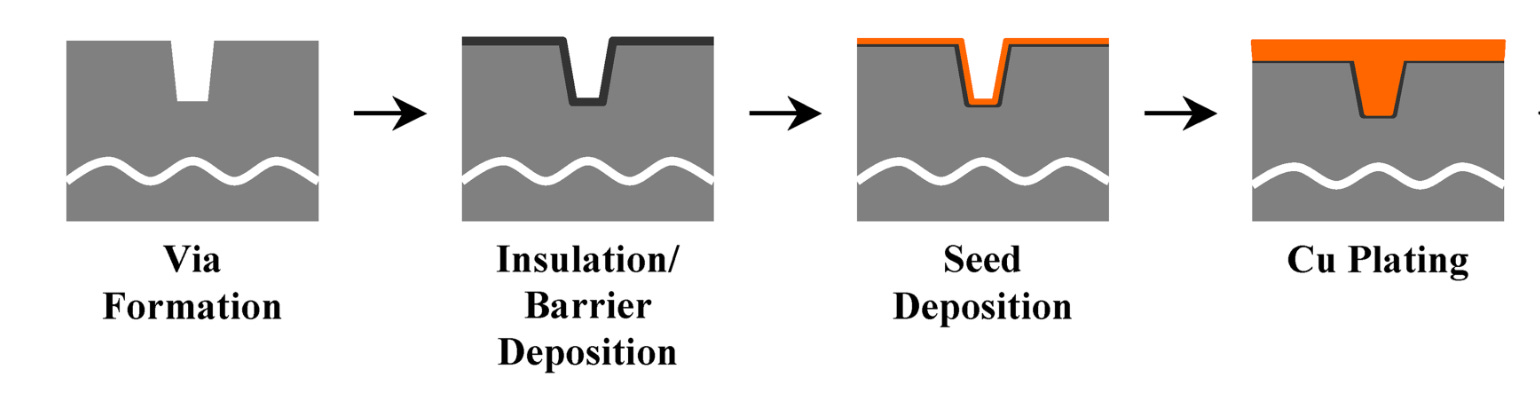
The difficulty lies less in pushing physics to its limits to reach such tiny dimensions than in managing the complexity of drilling deep into a chip with different materials and structures. At a basic level, the process involves carving a hole in a chip, depositing a thin layer of insulating material on top, and filling the rest with conductive copper.
A diagram of the TSV formation process steps from Applied Materials
Once the trench is complete and the copper wire is formed, a sequence of steps removes the excess material and flips the wafer to remove material on the other side, revealing the end of the wire. This leaves a TSV that runs through the whole memory die, making it ready to be stacked on top of other memory dies to form HBM. That process of carving away excess material, called chemical mechanical planarization (CMP), will be the subject of the next piece in this series, but for now, the focus is on etching the TSV trench and filling it with copper.
Given that TSVs are much larger than memory capacitors and that China has already been making significant gains in its etching capabilities, etching is unlikely to be a bottleneck for China to produce TSVs. While TSV etching differs in some important ways from capacitor etching—notably, it is a multi-step process rather than a single step—it is unlikely to pose a major challenge. TSV etching machines from AMEC and Naura can meet the needs of China’s HBM production, and exceed the TSV etching limits that are built into US export controls.3
Overall, several types of SME are needed to produce TSVs:
Photolithography tools to pattern where to etch the TSVs
Etching machines to carve out the TSVs
Deposition machines to fill in the desired materials
Cleaning tools to remove unwanted impurities
Chemical mechanical planarization and other grinding tools to shape the wafer
Metrology tools to measure these various processes and keep them on track
Photolithography is an extremely important bottleneck for much of China’s semiconductor production, but it is not especially significant here. Given the large feature sizes of TSVs, they do not require precise lithography and can therefore rely on lagging-edge tools that China has in relative abundance and can still import from ASML, Canon, or Nikon.
Etching machines are unlikely to be a bottleneck for similar reasons: the large feature sizes of TSVs. Cleaning tools are an area of relative strength for China, with ACM Research, the focus of the latter half of this piece, having built a globally competitive portfolio.
This leaves deposition machines, chemical mechanical planarization, and metrology tools. All three are important potential bottlenecks and will be the focus of this and subsequent pieces in this series, starting with deposition tools, the next step in the TSV formation process after etching.
China can handle the needed thin-film deposition
Deposition is the process of placing material onto the wafer. Like etching, it comes in a wide variety of forms, as a vast array of processes, materials, and structures require different deposition techniques.
For producing TSVs, there are four key deposition steps. The first three can be grouped together as they are all variations of thin-film deposition; the fourth, copper electroplating, works differently and is discussed below.
Sourced from “Tutorial on forming through-silicon vias” in the Journal of Vacuum Science & Technology.
The first three deposition steps place thin layers of different materials on top of one another. The first is an insulating layer that stops electrical interference between the conductive substrate and the copper wires. Next, a barrier layer is needed to stop copper atoms from diffusing through the insulator into the surrounding silicon, damaging other structures on the chip. Finally, a “seed” layer of copper is applied, acting as the base for the electroplating stage.
These thin-film deposition tools are an area where China lags behind the technological frontier, though for TSVs, this gap is not particularly relevant. Since TSVs are large and use well-established materials, they don’t require cutting-edge thin-film deposition capabilities. Thin-film deposition is unlikely to be an important bottleneck for China’s HBM production. (The appendix below gives more information on how thin-film deposition works and the reasoning behind that view.)
Few Chinese firms are developing electroplating
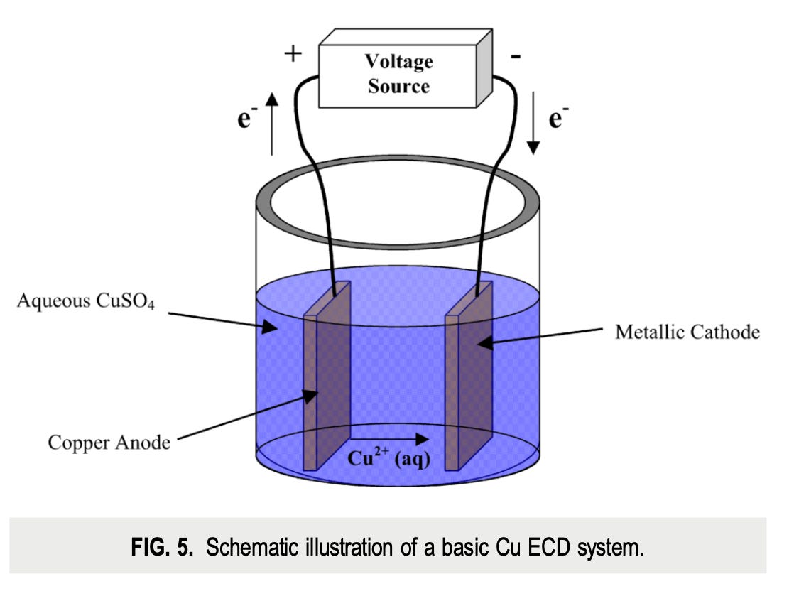
Once these various linings are in place, the challenge is to fill the rest of the TSV with copper. This process is called electroplating or electrochemical deposition. Electroplating uses electrolysis, in which a circuit is established between a cathode and an anode. This oxidizes copper at the anode, sending electrons through the external circuit and releasing positively charged copper ions into the solution; at the cathode, the ions meet those electrons and are reduced to solid copper on the surface. The same process is used to plate gold or silver jewelry: a ring is placed in a solution containing dissolved gold, and a current is passed through it, depositing a layer of solid gold. With TSVs, this happens on a microscopic scale.
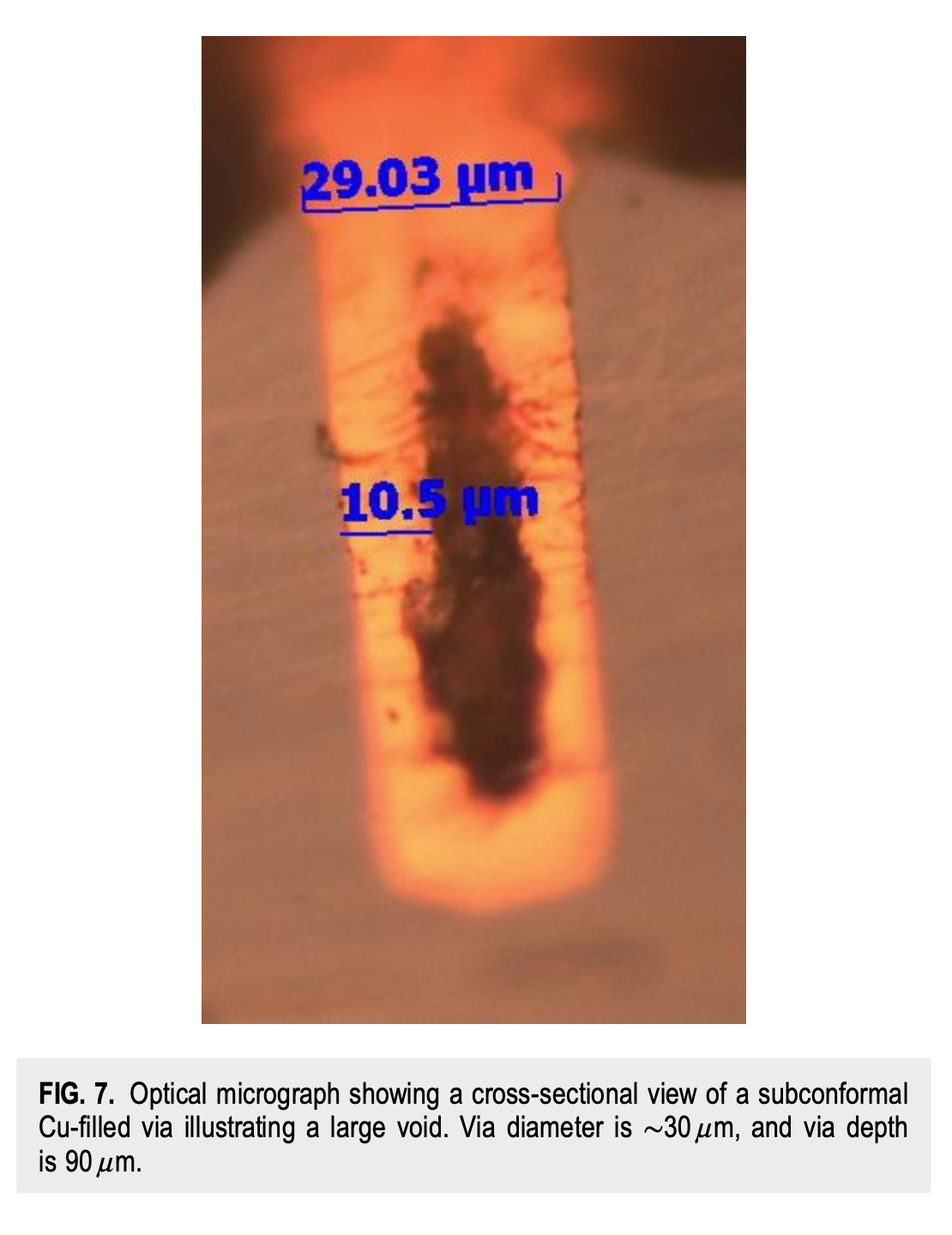
The diagram on the left shows a simple version of how copper electroplating functions; the image on the right shows the difficulty of electroplating with an Eye-of-Sauron-esque void having formed within the copper, both from “Tutorial on forming through-silicon vias” in the Journal of Vacuum Science & Technology.
In the TSV, the deposited copper seed layer acts as the cathode, meaning copper continually builds up on it, slowly filling the space. The complexity comes in managing the pace at which this copper forms, and where within the TSV. A bottom-up fill is needed, as one key issue is voids forming within the copper (as shown above). These are holes within the copper, formed by impurities, trapped air, or mismanagement of the deposition process, in which the top of the TSV fills before the bottom does.
China has a few makers of electroplating tools, with only ACM Research having a range of machines, the first released in 2019.4 Naura entered the market in March 2025, with an electroplating machine for TSVs.5 Therefore, much more so than in thin-film deposition, China depends principally on the capabilities of a single firm, with Naura playing a secondary catch-up role.
The Ultra ECP 3d meets China’s TSV electroplating needs
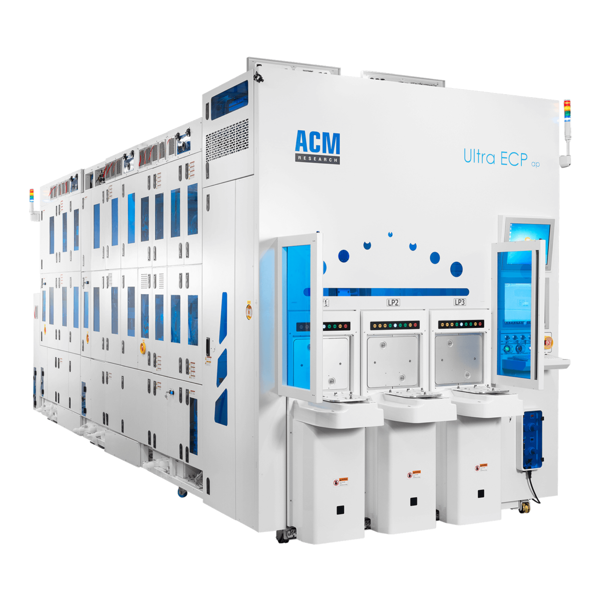
ACM Research’s electroplating offering for TSVs is the Ultra ECP 3d. For some odd reason, the listing of the ECP 3d on ACM Research’s website shows a picture of a different machine, the ECP ap, which is a less specialized electroplating machine for packaging processes. Even more displeasing, it fails to capitalize the D in “3D”.
ACM Research describes the ECP 3d like this:
Building on our proven electrochemical plating (ECP) technology, the Ultra ECP 3d is configured with ACM’s exclusive Multi-Anode Partial Plating function, which allows the deposition of the copper metal layer on via structures of 3D TSVs and 2.5D interposers, and is compatible with aspect ratios of 10:1 and beyond.
The Ultra ECP 3d is likely capable of handling the electroplating steps necessary for China to fill TSVs to produce HBM. The metrics and descriptions given by ACM Research suggest that it is operating at a fairly advanced level.6 For instance, the ECP 3d has multiple anodes to better control how material is deposited, and ACM claims it can handle aspect ratios of 10:1 and above.7 That would make it suitable for the TSVs needed to produce HBM.
Electroplating is not a step that pushes the cutting edge of semiconductor physics, so unsurprisingly, ACM Research can produce a tool for the job. The differentiator for US tools produced by Lam Research and Applied Materials lies not in capabilities but in performance. High throughput, high uniformity, and good integration with other systems throughout the fab almost certainly still make their machines more attractive to chip makers than ACM Research’s would be.
Assessing the gap in these metrics is very difficult due to the lack of publicly disclosed information from these SME companies. Marketing materials usually give vague allusions to capabilities—“50% faster” or “higher uniformity”—but no concrete information. One concrete comparison is the timing of the tools’ introduction. Lam Research’s current platform was introduced in 2015, with Applied Materials following in 2017, and ACM Research in 2020. Lam Research was first and is the clear market leader.8
Lam Research, with a platform in use at leading memory firms since 2015, benefits from over a decade of iteration and knowledge of the cutting edge of HBM production. That translates into higher performance across commercially important metrics such as throughput and yield. ACM Research has had less time, shipped fewer machines, and worked with less sophisticated customers, and so will likely perform worse on these commercial metrics. Even if its machines are technically sophisticated enough to produce the needed TSVs, they likely do so at significantly lower yield.
While the Ultra ECP 3d having the basic capability is a necessary step, raising yield is a top priority, especially for China’s HBM efforts, which already face numerous technological bottlenecks and yield issues elsewhere.9 Since a silicon wafer goes through hundreds and hundreds of process steps before becoming a completed chip, low yields at any point in the process can wreak havoc on the overall output. Sufficiently low yields can render an entire product line uncommercial or cause extensive delays, as chip makers need more time to consistently iterate and gradually raise yields to acceptable levels.
ACM Research very likely still lags Western machines on these yield and performance metrics. By how much, and to what effect on China’s overall HBM production, is hard to assess and a question I’m still trying to answer. My best estimate is that electroplating is unlikely to be a major source of poor yield in China’s HBM process, and that ACM Research is only a few years behind Lam Research or Applied Materials in the performance of its machines. Electroplating is a relatively mature and stable platform for both Lam Research and Applied Materials, and a niche corner of the market, so it likely has not attracted major R&D efforts or technological upgrades. The primary benefit these firms have is a backlog of production data and iteration with chip makers, but ACM Research is likely to build this data quickly as Chinese memory firms look to rapidly scale their HBM production. ACM Research has also run this playbook before, initially entering the more niche and unloved market for wafer cleaning tools, and has since come to match the leading global suppliers.
ACM Research has reached the frontier before
ACM Research started with a bad idea. Its founder, Dr. David Wang, created ACM Research in 1998 with the vision of developing a copper-polishing tool that ultimately proved to be a dead-end. But the company’s fortunes were made by a better idea of pivoting into wafer cleaning tools, and an even better idea of establishing a subsidiary in Shanghai in 2006.10 Over time, ACM Shanghai has become the company’s core in R&D, manufacturing, and sales.
ACM Research, the parent company, remains headquartered in the US, which sometimes places the firm in uncomfortable positions. In December 2024, the US placed ACM Shanghai and its subsidiary in South Korea on the Entity List. This restricted its access to overseas markets for components. Despite strong revenue growth, ACM Research’s net income fell in 2025 as it incurred costs to rejig its supply chain and design out foreign-sourced components.
ACM Research’s growth has primarily come from its success in wafer cleaning products. As silicon wafers are repeatedly bombarded with energy, dunked in chemicals, and moved between extremely sensitive machines, there are many ways that impurities can upset the process. ACM Research built its capability here through the 2010s; the major breakthrough came in 2013, with a contract to supply Korean memory maker SK Hynix for one of its fabs in China.
ACM Research has created cleaning products comparable to those from Japanese players Screen and Tokyo Electron, as well as US-based Lam Research.11 It has closed this gap enough to become the dominant provider in the Chinese market, with its largest customers being Chinese memory makers YMTC and CXMT, as well as logic manufacturer SMIC.
ACM Research has also made innovations of its own by finding a niche in megasonic acoustic vibrations, which can aid in cleaning processes but also risk damaging the features built on the chip. This innovation is helping make it globally competitive. One indication is that Intel has tested ACM Research machines for potential use in its upcoming and most advanced 14A process. Given the risks posed by using China-sourced equipment and the strong pushback Intel has received from US lawmakers, it seems unlikely that ACM Research’s tools will be used in Intel’s fabs. But that an important global chip maker would be interested reflects impressive technical sophistication.
Beyond cleaning and electroplating, ACM Research’s ambitions are quite galaxy-brained. At Semicon Shanghai, it announced a refreshed product portfolio that maps its various platforms to planets.
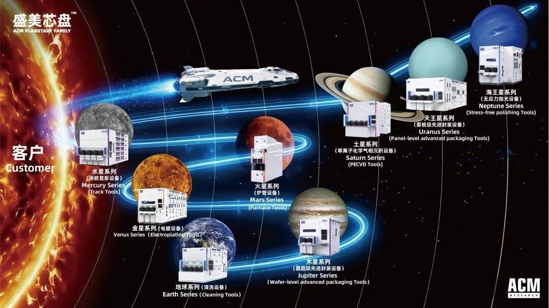
A promotional image from ACM Research’s official WeChat account.
The explanation behind the branding refresh is not lacking in grandeur:
As humanity gazes up at the vast starry sky, from exploring celestial bodies to intelligent algorithms, a microscopic revolution in the global arena is rewriting the course of human civilization. Today, humanity’s pursuit of computing power has transcended Earth’s surface, venturing into the vast outer space. This relentless spirit of exploration is the core mission that drives ACM Research’s deep commitment to semiconductors and continuous innovation—and also the inspiration behind our Eight Planets product series.12
If sometimes perhaps a little overwrought:
ACM Research has always been customer-centric, maintaining our core position like planets orbiting the sun, with unwavering centripetal force and singular focus, providing the highest quality and most considerate service. Customers are like the sun, providing us with light and warmth.13
TSV formation is not a strong bottleneck to China’s HBM production
China has reasonably capable domestic tools across the various etching, thin-film deposition, and electroplating steps needed to form TSVs. The open question is whether Chinese HBM producers can achieve yield at scale, not whether the tools themselves will be available. Given the relatively modest dimensions and material simplicity of TSV formation compared to advanced logic or memory production, it is unlikely to be a strong bottleneck for China’s indigenous HBM production.
Access to Western TSV tools would help China on the margin by improving yield, but their restriction would not impose a strong chokepoint effect. Yield matters greatly, with current industry rumors suggesting that Chinese memory maker CXMT is struggling to get viable yields on its HBM production as it tries to scale it up this year.14 Importantly, this is while CXMT’s HBM production currently relies principally on imported Western tools rather than on Chinese domestic equivalents. Even as Chinese SME firms close the gap in tool capabilities, there are plenty of other challenges in the required material inputs, process integration, and yield learning.
The truly strong bottlenecks remain in the most advanced tools for cutting-edge logic and memory production, with lithography tools the most important. While further restrictions on TSV etching and deposition tools would impose costs by harming China’s HBM yield, restricting DUVi lithography tools will effectively forestall China’s ability to build out incremental advanced-node capacity. No more DUVi means no more advanced DRAM, which ultimately means China cannot scale up HBM production. The prioritization of DUVi restrictions within the MATCH Act over TSV tool restrictions is therefore not a cause for concern.
Appendix
Thin-film deposition
The various thin-film deposition steps involved in TSV formation use three different techniques:
Chemical vapor deposition (CVD) works by triggering chemical reactions between the substrate and an energized gas, leaving the desired deposition material as a byproduct. Chemical vapor deposition needs energy to trigger the necessary reactions; in basic chemical vapor deposition, this is thermal energy from high temperatures. However, one of the challenges of producing TSVs is that they are usually not the first feature to be built, which means high temperatures could damage the already constructed transistors or capacitors. This is why plasma-enhanced chemical vapor deposition is necessary: the plasma provides some of the energy needed to produce the reactions, reducing the required temperature.
Physical vapor deposition (PVD) works by placing the surface to be coated into a vacuum chamber facing a chunk of the material to be deposited. This material is then bombarded with charged ions to break off particles, which, once free, are attracted by the clever use of electrical fields to form a layer on top of the target surface.
Atomic layer deposition (ALD) uses heat or plasma to drive reactions between a gas and the wafer surface. The difference is that with atomic layer deposition, these reactions are done one layer of atoms at a time. This makes the process more time-consuming but allows for much higher conformality, meaning that the deposited material is spread exactly evenly over the desired surface.
China likely has sufficient capabilities in all three to handle the creation of TSVs. Due to TSVs’ large feature sizes and the use of relatively standard materials, the thin-film deposition required is not close to the technological frontier. China’s tools can lag significantly behind those used by Western firms for advanced logic and memory nodes, where feature sizes are much smaller, and a wider range of materials is required.
This is reflected in US export controls, which target advanced tools for logic and memory fabrication rather than the lagging-edge TSV-capable tools considered here.
The relevant tools are now produced by a set of Chinese firms. Naura produces CVD, PVD, and ALD tools, while Piotech and AMEC both produce CVD and ALD tools. Supply chain data from the Center for Security and Emerging Technology shows Chinese deposition suppliers going from 1% global market share to 10% in 2024, a trend that will almost certainly continue, as Naura and AMEC both posted strong deposition revenue growth through 2025.
SK Hynix cites 8,000 TSVs per die back in 2022 for its HBM3 production, which has since risen through HBM3E and now into HBM4 as the number of signal TSVs increases as the parallel I/O grows and as larger stacks likely require more power management from power TSVs.
SemiAnalysis cites memory capacitors as being “~1,000nm high but only 10s of nm in diameter” while Applied Materials gives 5 µm as a standard diameter for TSVs. One µm is 1000nm, so a 5000nm TSV is 200 times larger than a 25nm capacitor.
See Aqib Zakaria’s great ChinaTalk piece, How Far Can Chinese HBM Go?, where he concludes that TSV etching machines from Naura and AMEC already have the requisite specs for the relevant SME item control 3B001.c.4.
See the ‘New Product Information’ in this ACM Research Q1 2019 financial report, which references the release of its first ECP tool.
See the coverage of Naura’s R&D roadmap here which gives the specific date of its ECP machine’s release.
Multi-anode features and partial pulse plating are both more advanced electroplating techniques, and the figures given on uniformity seem relatively strong but are hard to assess due to a lack of comparable figures from other firms.
See the product description on ACM Research’s website, the aspect ratio is the ratio of the height to the width of the feature, in this case TSVs are ten times as deep as they are wide.
Lam Research cites in its Q1 2023 earnings presentation “100% market share for SABRE 3D and Syndion systems across leading memory customers for TSV formation”.
For instance, China cannot access EUV lithography machines, which are used at the most advanced memory nodes, forcing it to instead rely on older DUV immersion machines and a process of multi-patterning where the wafer goes through more exposures, creating greater yield challenges. China is similarly restricted from various other advanced etching, deposition, and metrology tools, with its domestic substitutes usually not as mature as those from leading global SME firms.
See this SemiAnalysis piece for an account of ACM Research’s early history.
See this piece on ACM Research from SemiAnalysis on how it stacks up against peers.
Translated from ACM Shanghai’s announcement on its official WeChat account by Claude Opus 4.6, the original Chinese is “当人类仰望浩瀚星空,从探索星辰到智能算法,一场微观世界的全球革命,正在改写人类文明进程。当前,人类对算力的追求已然超越地球表面,迈向更广阔的地球外太空。这份永不止步的探索精神,正是盛美深耕半导体、持续创新的初心,也是我们打造八大行星系列产品的初衷”.
Translated from ACM Shanghai’s announcement on its official WeChat account by Claude Opus 4.6, the original Chinese is “盛美始终以客户为中心,如行星绕日般坚守核心、精准同向,以恒久不变的向心力与极致专注,提供最优质、最贴心的服务。客户如同太阳,赋予我们光与热”.
See Aqib Zakaria’s recent ChinaTalk piece on whether the US should buy memory from CXMT , where he assesses various rumors about CXMT’s yield on its HBM and discusses what that would mean for its profitability.
 | A guest post by
|