

China is making strides in etching machines for memory
AMEC’s current etching machines can’t support China’s high-bandwidth memory efforts, but its next flagship likely can.
This is the first piece in a series exploring some of the key semiconductor manufacturing equipment that China needs to indigenously produce high-bandwidth memory, perhaps the most important bottleneck to its efforts at making AI chips.
For China to manufacture high-bandwidth memory (HBM)—a key component of advanced AI chips—at scale, it must overcome a complex web of dependencies on non-Chinese semiconductor manufacturing equipment. One key bottleneck is in advanced etching machines, crucial for producing the dense memory cells that latest-generation HBM requires. China’s best machine here, AMEC’s Primo UD-RIE, is likely six to eight years behind the frontier, though AMEC is working on a successor that could narrow the gap to two to three years.
Whether AMEC can deliver matters greatly for China’s ability to scale HBM and therefore broader AI chip production. CXMT, China’s leading HBM producer, likely has enough imported etching machines to produce HBM3—two generations behind the frontier but still significant—but due to export controls its ability to keep scaling HBM production through 2026 and into 2027 will increasingly depend on domestic Chinese etching machines. Currently the Primo UD-RIE is not good enough for HBM3 production, but the promised successor likely would be.
AMEC has been growing rapidly, including with its R&D spending, and is working along established pathways of technical development. Because of this, I expect it will be able to largely solve this bottleneck to China’s HBM production. In this post, I first explain the basics of memory and etching, then examine the Primo UD-RIE and AMEC, and finally conclude with what the analysis means for China’s overall AI chipmaking efforts.
China is advancing in etching but remains years behind the frontier
The Primo UD-RIE is made by Advanced Micro-Fabrication Equipment Inc. (AMEC), a leading Chinese provider of etch and deposition equipment.1 I could find only a single grainy image of the UD-RIE:
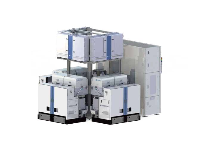
A visualisation of the UD-RIE from the product page on AMEC’s website.
AMEC describes the UD-RIE as
a high-end capacitive coupled plasma (CCP) etch system developed by AMEC based on its own IP. Specifically designed for the most critical high aspect ratio (HAR) dielectric etching process for memory device fabrication.2
That is a rather dense technical description, so let me walk through what it actually means.
Memory is essential to AI chips
A logic chip, such as an AI chip, processes information, with the results stored and accessed in memory chips. Taking information from memory, processing it, and putting it back is the core loop that AI chip makers want to speed up to push computational performance.
AI’s demand for memory is voracious, with prices in some cases expected to double just in the first quarter of this year, pushing up costs for consumer electronics such as laptops and smartphones.
Memory comes in various flavours that trade off speed against capacity and other factors. The most important here is dynamic random-access memory (DRAM). DRAM is a workhorse that uses a simple structure to be scalable, fast, and relatively cheap. The trade-off is that DRAM is volatile—it loses its stored data over time or when it loses power—while other kinds of memory are persistent but slower or costlier.
Each cell of DRAM has just two components, a transistor and a capacitor. A memory cell stores a bit of information (a one or a zero) and retrieves it when needed. The capacitor stores this information as electrical charge. The transistor controls access to the capacitor. When the information is needed, the transistor opens the capacitor, and by measuring how many electrons flow out the value can be retrieved—if it was full of electrons it was a one, if it was empty it was a zero.
Today’s AI chips are so memory-hungry that the DRAM used in phones and laptops is insufficient. It simply does not offer enough capacity for frontier AI models and the data that goes along with them. The solution is high-bandwidth memory, or HBM. Making HBM involves placing specialized DRAM chips on top of one another—up to 16 in the latest generation—to form an HBM stack. This stack is placed alongside the logic die as close as possible, since distance matters even at such miniature scales. The magic of HBM is how these DRAM chips are connected with through-silicon vias—wires cutting through the layers of DRAM to form vertical communication highways—that allow as much information as possible to flow to and from the memory.
DRAM is a likely bottleneck to China’s HBM production
The building block of HBM is high-quality DRAM, which packs as many cells as possible into the smallest area. Producing large volumes of advanced DRAM requires expensive equipment and sophisticated R&D. The market has historically been highly commoditized, with huge boom-bust cycles that have whittled down the number of global players to just three: Samsung and SK Hynix of South Korea and Micron of the US. Though CXMT has been gaining ground, it is still sitting at 4% (and growing) market share in mid-2025, versus the 90% of the big three combined.
Producing cutting-edge DRAM poses distinct challenges compared to other areas of chip making. For a logic chip, the greatest difficulty is cramming ever more transistors—the tiny switches that flip between ones and zeroes—into each square inch. The main bottleneck for doing so is lithography, where extremely precise light is used to create patterns on the silicon wafer to form these minuscule transistors. With DRAM, the hurdle is instead the capacitors that store electrical charge.
As capacitors were shrunk ever smaller, storing enough electrons in them to detect the tiny signal fluctuations when reading a one or zero became increasingly difficult. Capacitors could keep shrinking horizontally only by stretching vertically to maintain enough electron storage. Capacitors therefore now look like extremely skinny tubes stretching up from the chip surface. This verticality presents different challenges from shrinking transistors, and the key process for making these tall, fragile capacitors is etching.
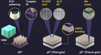
This diagram, courtesy of Lam Research, shows the evolution of DRAM layouts. Notice the tall skinny capacitors in 6F² and how these become even skinnier and denser into 4F².
Etching is vital to producing advanced memory
Etching is a core process in both logic and memory chip production. Starting with a silicon wafer, the process alternates between depositing material, using photolithography to sketch patterns, and using etch machines to remove unwanted material. By repeating this cycle, along with numerous other steps such as cleaning and measurement, the structure of a chip is built up.
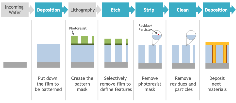
This diagram, from Lam Research, gives a good breakdown of the various core process steps involved in producing a chip.
Etching machines come in many varieties depending on the method, the material being etched, and the features desired. The tall, skinny capacitors needed for DRAM require a plasma etching machine. These are also known as “dry” etching machines, as opposed to “wet” etching machines that use liquid chemicals.
A plasma etching machine takes in various types of gasses, then uses a powerful radio frequency source to accelerate free electrons, so that they smash into the particles of these various gasses. This breaks the molecules into ions, radicals, and more free electrons.
The new free electrons sustain a chain reaction that makes the plasma self-sustaining. The radicals are incomplete chunks of the previous molecules, and so are desperately seeking new atoms to become whole, making them chemically reactive. The ions are charged and can be directed by the electric field to collide with the material to be removed (a process known by the oddly whimsical name of “sputtering”). The combination of physical bombardment and chemical reactions speeds up material removal, and is termed “reactive ion etching”.
Etching capacitors requires three further things:
The etching machine must be designed for dielectrics. A wide variety of metals and chemicals are used at different stages of chip making. For capacitors the material is dielectrics—electrical insulators that polarise in response to electric fields, making them ideal for storing charge.
The machine must be specialized for high-aspect ratios. This is the ratio of height to width, which given the capacitors’ slender structures means ever-higher aspect ratios, reaching up to 100:1 for the most advanced DRAM.3
The machine must be powerful. Reaching the bottom of these high-aspect-ratio holes and continuing to remove material requires high-energy ions. The machine that best delivers this is a capacitively coupled plasma (CCP) tool, which uses a single high-powered radio frequency source, as opposed to inductively coupled plasma (ICP) tools that use multiple sources for greater control.
The Primo UD-RIE is likely 6-8 years behind the frontier
Now you should be better able to understand what the UD-RIE does, and why it is named what it is. I don’t know where “Primo” comes from, but “UD-RIE” seemingly stands for “ultra-deep reactive ion etch”.4 The product description should now also make more sense: a “capacitive coupled plasma etch system … designed for the most critical high aspect ratio dielectric etching process for memory device fabrication”.
To be effective at producing advanced DRAM, an etching machine must perform well across several metrics: how fast it can etch, how uniformly, how selective it is in etching only the right materials, and whether it can avoid defects and produce at high yields. Ideally one would have quantitative data on all these dimensions. Unfortunately, how these metrics trade off against one another is the secret sauce behind how effective these machines are, and so companies are loath to disclose any useful information at all. This makes rigorous comparison of how the Primo UD-RIE stacks up against Western equivalents difficult. Without private information, the best available approach is working from what published specs there are.
For the Primo UD-RIE, by far the most useful piece of information disclosed is that, in AMEC’s financial reporting, it describes the UD-RIE as being capable of 60:1 aspect ratio etching. Using that figure I very roughly compare it to equivalent machines from Lam Research and Tokyo Electron. My best estimate is that the UD-RIE is comparable to Western tools from 2018 or 2019, and remains well behind the most cutting-edge tools, which are now approaching >100:1 aspect ratios.5
What does this mean, concretely, for China’s HBM efforts? DRAM fabrication progress is usually measured in “memory nodes”, which are generations similar to the 4G and 5G of cellular networks. Each node builds on the one before to create ever denser memory cells and higher performance. Unhelpfully, memory nodes use confusing alphabetical naming conventions that have diverged between South Korean and American producers, but you can see the progression in the table below. HBM generations are similar, representing the progression to ever-higher HBM stacks that boast greater capacity and bandwidth.
The Primo UD-RIE is likely only capable of producing HBM2, or possibly HBM2E, some three to four generations and six to eight years behind the frontier. While supporting HBM2 production has some limited utility for China’s AI efforts, what China really needs is a machine that can support HBM3 production at scale. Huawei’s Ascend 910C has used a combination of HBM2E and HBM3, and Huawei has said it will adopt a custom HBM solution for its next line of Ascend 950 chips, but for this solution to be “more cost-effective than HBM3E and HBM4E” as Huawei claims, it will need production capabilities similar to HBM3.
China’s leading DRAM producer CXMT has targeted HBM3 as its goal for 2026, and will likely succeed at reasonable scale, due to its stockpile of advanced Western machines. Due to export controls limiting further import of these Western machines, CXMT needs domestic machines to scale up its advanced production and HBM3 into 2027 and 2028.
AMEC has promised that it can solve this bottleneck with a successor to the UD-RIE that can handle 90:1 aspect ratios. AMEC claims this machine is “about to enter the market”6 as of its most recent reporting, for Q3 2025. If true, this would be a major jump in capability, from six to eight years behind the frontier to more like two to three, covering more recent DRAM nodes including those needed for HBM3.
Producing an etching machine closer to the frontier will require AMEC to master a set of technical challenges that grow more extreme with each increase in aspect ratio. Reaching the bottom of ever taller and narrower holes to carve out capacitors needs better control across the radio frequency power source and the plasma itself. Controlling temperature becomes crucial, with effective etching requiring management of hundreds of temperature zones across the wafer, since some areas etch faster than others.
The key inputs to AMEC’s success here are R&D funding, strong human capital, and time, of which it has at least two.
AMEC is rapidly scaling its R&D spending
AMEC has become one of China’s largest semiconductor equipment companies, with products spanning etching, deposition, and other processes. Its origins trace back to early state industrial policies. It was founded by Gerald Yin in Shanghai in 2004. At age 60, Yin had established himself in Silicon Valley, graduating from UCLA and working for two decades at Intel, Lam Research, and Applied Materials.7 He returned with a team of 15 engineers to embark on the novel challenge of building a semiconductor equipment business in China.
AMEC produced its first etching machine in 2007, and attracted state attention and support soon after. In 2008, it was selected for the 02 Special Project, a major industrial policy effort aimed at indigenizing semiconductor manufacturing equipment, and in 2014 it was the first investment by the Big Fund, China’s leading state semiconductor investment vehicle.8
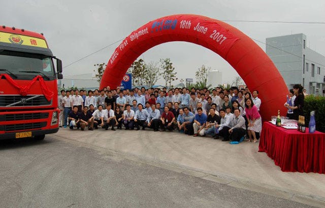
The weather looks dreary but at least they have the sparkling wine, via AMEC.
This continued open capital spigot has helped turn AMEC into a significant force in the Chinese market. While AMEC had more international presence earlier in the 2010s, it has become increasingly domestically focused, with 95% of its 2024 revenue from mainland China, a share that continues to rise.
The company’s mission is fairly clear. This, for instance, from Gerald Yin, who is still chairman and CEO, in the most recent semi-annual report, for H1 2025:
Due to the severe international geopolitical situation, we must urgently address our shortcomings and catch up. In H1, the company continued to invest heavily in new product R&D, with R&D spending reaching RMB 1.492 billion, up approximately 53.70% year-on-year.9
AMEC aims to cut its product development cycles from three to five years to two or less, and has 20 new models in R&D as it seeks to become a platform company spanning most of the semiconductor equipment space. Just over half of its total employees are R&D personnel, far higher a share than at its Western peers.
Despite this rapid growth, AMEC’s spending remains well below global leaders such as Lam Research in absolute terms. Lam spent $2.1 billion on R&D in its 2025 fiscal year, where AMEC looks set for $400-450 million. AMEC’s advantage is in pursuing a known technological path, rather than needing to push the frontier. Given continued state support for the industry and AMEC’s commercial success, it looks set to keep growing this R&D spending figure. Given enough time, I expect AMEC can catch up to the frontier in etching, perhaps by the early 2030s. What export controls have done however is bring forward the point at which China needs AMEC to be delivering comparable capabilities.
AMEC’s efforts likely solve an important bottleneck for China
HBM is crucial to China’s AI efforts, and is currently the key bottleneck to Huawei’s AI chip efforts. Without sufficient HBM China cannot produce the AI chips it needs at scale, and faces an even steeper compute deficit versus the US. Producing that HBM relies on CXMT accessing enough advanced machines to continue raising production over the next few years. AMEC plays a key supporting role here.
CXMT wants to produce HBM3 indigenously at scale. The Primo UD-RIE does not give CXMT this ability, but it does provide a machine for CXMT’s less advanced production lines, potentially allowing it to reallocate some of its scarce imported equipment to HBM3 production.
But AMEC could prove most consequential by delivering the 90:1 aspect ratio successor to the Primo UD-RIE this year or next. This would support CXMT’s current most advanced production, and also enable it to scale production of HBM3. Producing large amounts of HBM3 would still leave China behind the frontier, which has already moved through HBM3E to HBM4, but it would keep China in the AI chip making game. Without large amounts of HBM3, China’s AI chip efforts would seriously suffer, as memory would remain a bottleneck on both the quality and quantity of chips it could produce.
Drawing on very scarce information, I would guess that AMEC can deliver small numbers of this 90:1 machine later this year or into 2027 and scale up to full mass production in 2027/2028. It has a large R&D budget and deep pool of human capital, as well as seemingly strong technological and commercial momentum. As of its most recent financial reporting, it had sold a cumulative 25 UD-RIE machines, a product first developed in 2022 and formally announced in 2025.10 This compares to the roughly 100 capacitively coupled plasma etching machines AMEC sells a year,11 and the thousands of etching machines generally that Lam Research ships each year.
25 UD-RIE sales is therefore a strong start for a new advanced platform. Importantly, the UD-RIE represents meaningful capacity being built at Chinese memory leaders CXMT and YMTC. These firms previously relied on Western machines, but export controls now give them a far stronger incentive to cooperate with domestic equipment manufacturers such as AMEC. Open collaboration and support from the skilled process engineering teams within these firms significantly boosts AMEC’s ability to advance their machines’ capabilities.
Etching has been AMEC’s largest commercial success, with rapid growth and a rising share of revenue. One of the best indicators of AMEC’s technical progress will be whether it can continue this positive revenue trend, and whether it continues to share information on a 90:1 aspect-ratio machine, including breaking out specific sales figures. On its current trajectory, AMEC looks set to become one of China’s dominant semiconductor equipment firms and to plug vital gaps in China’s capabilities, such as etching machines for DRAM.
The rest of this series will explore more of these machines and the firms that produce them. The next post will look at the machines necessary for the crucial through-silicon vias—special wires that cut down through the layers of DRAM within HBM to make communication highways—that allow as much information as possible to flow to and from the memory.
Appendix
How advanced is the Primo UD-RIE?
My estimate is that the UD-RIE is comparable to Western tools from 2018 or 2019, and remains a ways off from the most cutting edge tools which are moving towards handling >100:1 aspect ratios. This estimate is pieced together from several sources, since no definitive public benchmark exists. Tokyo Electron, in its 2025 and 2022 investor day presentations, provides DRAM technology roadmaps citing aspect-ratio figures for capacitors at various memory nodes. Naively, these figures consistently undershoot those from other industry sources, such as SemiAnalysis’s claim of leading companies approaching 100:1 for recent nodes.
I think this disparity is likely caused by Tokyo Electron reporting the structural aspect ratio (the actual ratio of the finished capacitor), rather than the etching aspect ratio (what aspect ratio the etching machine needs to handle to produce that final capacitor). Given that during etching the capacitor will have a mask layer raising its height, and the hole tapers as it deepens, the effective aspect ratio needed during etching is higher than the final structural aspect ratio of the capacitor.
A very rough Claude-assisted estimate is that if the mask adds 30% to the height of the capacitor, and you take the critical dimension at the bottom of the capacitor hole as 0.75x the opening, then you can take 1.3 ÷ 0.75 to get a 1.7x differential between the capacitor aspect ratio and the etch aspect ratio. Given that, you would expect the Primo’s 60:1 etch aspect ratio to translate to a 35:1 capacitor aspect ratio, which on the TEL roadmap would place it around 2018 or 2019.
It is possible that AMEC’s aspect ratio claims could be mapping more to NAND than DRAM as another source of the disparity, but I can’t verify this because I can’t find good public sources on the differences between NAND and DRAM aspect ratios. Sources often refer only to aspect ratios for advanced memory, not specifying NAND or DRAM despite the quite different feature profiles between them. If you can point out the (likely) errors in this analysis please do get in touch! I would like to better understand the details of the differences between DRAM and NAND etch.
Another way of estimating the capabilities of the Primo UD-RIE is via its listed features, though these are somewhat vague. The UD-RIE has features such as active edge impedance tuning, multi-level radio frequency pulsing and active by-zone temperature control that became standard during the mid-to-late 2010s. Notably, it does not have cryogenic capabilities that have become a key focus of Lam and Tokyo Electron during the 2020s for pushing the frontiers of NAND.
Why the Primo UD-RIE can’t be used for CXMT 1z production
The UD-RIE is likely not sufficient for CXMT’s 1z production, due to CXMT moving from 6F² to 4F² for its 1z production according to SemiAnalysis. What this means is that CXMT is shrinking down the overall footprint of the DRAM cell, by fitting the transistor underneath the capacitor, rather than having it sit alongside. This gives a significant boost to memory density as you no longer need to focus on shrinking down the transistor even further to shrink the overall DRAM cell.
Effectively CXMT is choosing a more challenging etching process as the best trade off to make given their limitations from a lack of access to extreme ultraviolet photolithography equipment. Opting for tricky vertical structures over smaller transistors. Since doing this raises the aspect ratios needed for 1z significantly above what they would otherwise be for a 6F² layout, the Primo UD-RIE is likely not up to the task, with CXMT instead relying on imported equipment and on AMEC shipping a 90:1 successor machine.
The two largest players in etch and deposition are AMEC and Naura. Naura is larger by revenue and produces a line of HAR dielectric etch machines with their Accura NZ that is similar to the Primo UD-RIE. Though Naura has disclosed less information on the Accura’s capabilities than AMEC has with the UD-RIE. This makes it difficult to properly assess which is the leader, but given Naura came to dielectric etch later than AMEC (only beginning in 2021 vs early 2010s for AMEC), and has shipped far fewer CCP systems, it seems likely that AMEC is closer to the cutting edge.
See the Primo UD-RIE product page on AMEC’s website for the full product description and features.
HAR etch has generally been more significant in NAND than DRAM due to NAND having adopted fully 3D structures as early as 2014. DRAM has thus benefitted from tools pushing capabilities to be able to tackle increasingly HAR etch through many layers of stacked NAND. DRAM by contrast still uses 2D transistors even if capacitors have become vertical structures, with full 3D DRAM not expected until towards the 2030s. NAND generally requires much greater depth at lower precision, while DRAM faces shallower depth but needs higher precision.
AMEC does not clearly spell out the acronym but does describe it as “used for ultra-high depth-to-width ratio etch processes” (用于超高深宽比刻蚀工艺的), see their 2025 Semi Annual Report.
See the appendix for a full breakdown of the reasoning behind this estimate.
‘即将进入市场’, from AMEC’s Q3 2025 quarterly report.
See this Caixin Global piece on Gerald Yin’s background and the founding of AMEC.
From AMEC’s corporate history page which documents what AMEC considers key events in its development.
See pages 1-2 of the 2025 Semi Annual Report.
The specific claim is 200 cumulative UD-RIE chambers, where a single machine will have multiple chambers. The UD-RIE is advertised as having a “maximum six single wafer etch reaction chambers and two photoresist strip chambers” so 200 total chambers would be 25 machines assuming that AMEC is counting only the 6 etching chambers, and all machines have been shipped in the full 6-chamber configuration.
AMEC reports their cumulative CCP chambers shipped at various points. We know this figure was 4,500 in H1 2025, and 3,600 at the end of their Fiscal Year (FY) 2023 giving sales of 900 chambers over those 18 months, so 600 a year, which equates, given that most AMEC CCP machines have 6 chambers a tool, to 100 sales of complete machines a year.
 | A guest post by
|