

A forecast of Chinese DUV and EUV photolithography progress
What we can and can’t learn from ASML.
This post was written in collaboration between the AI Futures Project and The Substrate and cross-posted to both.
Restrictions on photolithography machines are a crucial bottleneck for China’s AI chip efforts. To get around them, China needs to replicate some of the most complex products ever built. Only the Dutch firm ASML has developed commercial extreme ultraviolet (EUV) machines after a decades-long effort, relying on a network of 5,100 suppliers; each EUV machine requires more than 100,000 components.
Whether China can indigenize photolithography machines is one of the central questions for future US-China competition over compute and AI. This piece uses the experience of ASML as a reference to argue that the late 2030s should be the anchor point for any forecast of when China produces commercial-scale EUV machines, and the mid 2030s for immersion deep ultraviolet (DUV).
Given these baselines, any forecast that puts either in the 2020s requires strong justification. This piece describes both how these baselines were derived and also considerations that push a forecast earlier or later: for example, how Chinese firms can learn from ASML’s technical pathway, the extensive state support behind China’s efforts, and the different starting positions for ASML and China’s sub-component ecosystems.
Photolithography is an essential step in semiconductor manufacturing: it uses a light source to transfer a pattern from a mask onto a silicon wafer. The difference between generations of photolithography machines lies in the precision of the light source and the size of the pattern it can produce.
The two types of photolithography of interest here are immersion DUV machines and EUV machines. Immersion DUV tools are a subset of DUV tools that place a layer of ultra-pure water within the machine to further focus the light. These machines are an older generation but still essential for many less precise steps in chip production, and through a technique called multipatterning, they can produce chips down to the 7 nm node.1 EUV machines are the most advanced, used for the most precise stages of semiconductor production.
The US pushed the Netherlands to block the sale of an EUV machine to China in 2019, and export controls have prevented any from entering since. China imported about 180 DUV machines between 2021 and 2024, though successive rounds of restrictions have blocked shipments of many advanced models and limited which Chinese chip fabrication plants (“fabs”) can legally import them.
Without sufficiently advanced domestic DUV machines, China cannot expand production at its most advanced node—currently 7 nm—except through imports that the Dutch government controls. It can still access immersion DUV tools under those controls, via the NXT:1980Di, but the MATCH Act, a Congressional effort, seeks to block this pathway. Without EUV capabilities, it cannot effectively pursue nodes below 7 nm, falling further behind global fabrication firms such as TSMC, which began 7 nm production in 2018 and is now producing chips at 2 nm.
Despite the importance of this question, there are few rigorous public forecasts. The Center for Security and Emerging Technology (CSET) ran a seven-person expert survey in 2021, but used vague wording.2 Forecasts by the RAND Forecasting Initiative and those on Metaculus are useful but sensitive to wording choices,3 and lack detailed qualitative reasoning or accompanying empirical data.
In 2024, ASML’s CEO suggested China was 10-15 years behind, and in March 2026, SemiAnalysis’s Dylan Patel predicted fully indigenized DUV tools and pre-commercial EUV tools by 2030. These public statements are useful but lack specificity. Take “pre-commercial”: ASML had EUV tools that could be termed pre-commercial from 2006 to 2019, when commercial production using its EUV tools began.
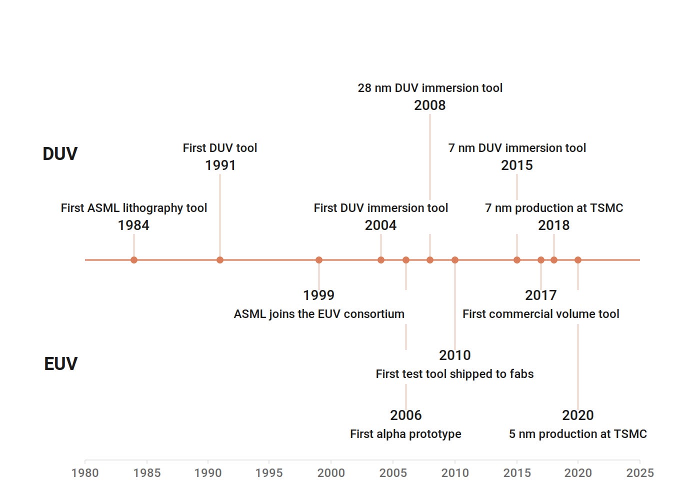
Timeline of ASML’s DUV and EUV development
What matters in forecasting progress in photolithography is whether large-scale commercial chip manufacturing happens—not whether a specific machine can produce functional light or a few working chips under controlled conditions. Commercial manufacturing is far more demanding and requires long periods of cooperation between the toolmaker and downstream chipmakers.
Two milestones in China’s indigenization effort are worth forecasting precisely. The first is domestic DUV machines capable of 7 nm production entering large-scale commercial use. The second is EUV machines capable of 5 nm and more advanced production entering large-scale commercial use. Both milestones are inflection points: DUV unlocks larger quantities of AI chips, and EUV unlocks large volumes of higher-quality ones.
A challenge in forecasting these milestones is that both have few relevant data points: ASML and Nikon for immersion DUV, and ASML alone for EUV. For immersion DUV, ASML has a 98.7% market share,4 so we only consider ASML here. For EUV, ASML is the only example, unless the reference class is extended to a broader, woollier category of complex technologies.
Still, ASML alone offers a great deal. EUV development in China will be similar to ASML’s efforts in many ways: pursuing innovations in optics and light sources, wrangling critical sub-component manufacturers, and undertaking extensive testing and iteration with chip makers. ASML’s experience gives good base rates—simple forecasts that anchor further analysis.
This piece sets out a methodology for deriving these base rates, presents the resulting forecasts for China’s lithography milestones, and then examines the other factors that shape a final, all-things-considered forecast. Finally, it surveys the current state of the art in Chinese photolithography and concludes with further research questions and key indicators to track.
The methodology behind the base rate forecasts
We use ASML’s experience to obtain base rates for when China will hit two photolithography milestones: commercial-scale 7 nm-capable immersion DUV lithography and commercial-scale 5 nm-capable EUV lithography.
To do this, we use two methods:
Industry-level development takes the time between when the global semiconductor industry began developing a technology and when it reached commercial maturity. It then adds this period to when China’s industry began developing the same technology to forecast when China will reach commercial maturity.
Product-level development takes our best sense of where China’s current indigenization efforts stand and matches it to the progression of machines ASML pursued. For instance, if China in 2025 had a machine comparable to an ASML machine from 2010, and it took ASML ten years to develop that into a milestone-relevant tool, the forecast would put China at that milestone in 2035.
These two methods are then applied to 7 nm capable immersion DUV and 5 nm capable EUV in turn. In each case, the right dates for the forecast parameters are uncertain, so we produce a range: a lower bound of the earliest date China might reach the milestone under that method, and an upper bound of the latest. We then take the midpoint as the median.
Industry-level forecasts
For immersion DUV, the upper and lower bounds are set by taking the gaps between:
When the global industry began DUV development, dated to 1988 with the first DUV R&D tool, and when it reached commercial 7 nm production with TSMC in 2018, a gap of 30 years
When ASML shipped its first krypton fluoride (KrF) DUV tool in 1991 and the same milestone of TSMC 7 nm production in 2018, a gap of 27 years
We then combine these gaps with various milestones from SMEE, which has historically been China’s leading photolithography firm, to establish an upper and lower bound. SMEE serves as a proxy for China’s semiconductor industry more broadly because large-scale industrial policy plans have shaped its development efforts:
We obtain a lower bound of 2032 by taking the 30-year gap from initial DUV development globally to 2018 commercialization, and adding this to a starting date of 2002, when SMEE was founded and integrated into the 863 Program industrial policy effort.
We obtain an upper bound of 2038 by instead taking the 27-year gap from ASML’s first commercial KrF DUV tool and adding this to SMEE’s first KrF tool in 2011.
We use the same method with EUV. We date the start of commercial EUV development to the formation of the EUV LLC consortium in 1997, and commercial EUV production to TSMC using ASML EUV machines for 5 nm production in 2020, giving a gap of 23 years. We then add this to two potential beginnings of China’s EUV development efforts to give bounds:
We obtain a lower bound of 2038 by adding the 23-year gap to a start date for China’s EUV efforts of 2015, the year of the “Made in China 2025” plan.
We obtain an upper bound of 2044 by adding the same 23-year gap to 2021 as the beginning of serious Chinese EUV efforts.5
Product-level forecasts
For immersion DUV, we set the bounds by identifying which ASML machine most closely matches China’s current level of development. We take the most advanced Chinese machine to be Yuliangsheng’s reported 28 nm prototype. We estimate this to be similar to ASML’s systems in 2007, two years before it shipped the NXT:1950i, the first immersion DUV tool in what would become its core DUV line.
It took ASML either 8 or 11 years to get from 2007 to a relevant milestone for 7 nm DUV: producing the 7 nm-capable NXT:1980Di in 2015, or TSMC beginning commercial 7 nm production in 2018. This gives:
A lower bound of 2033 by adding this 8-year gap to China’s current state of the art in 2025
An upper bound of 2036 by adding an 11-year gap to 2025
For EUV, we assess that China’s leading effort, the prototype machine reported on by Reuters, is roughly equivalent to ASML demo tools from either 2006 or 2008. This gives either a 12- or 14-year gap to TSMC’s first commercial 5 nm production using EUV in 2020. This implies:
A lower bound of 2037 by adding a 12-year gap to the 2025 EUV prototype
An upper bound of 2039 by adding a 14-year gap to the 2025 EUV prototype
Base rates suggest 7 nm capable immersion DUV by the mid-2030s and EUV toward 2040
A visualization of the base rate forecasts is below. For 7 nm capable immersion DUV, the forecasts cluster around 2035; EUV stretches out towards 2040.
The key takeaway is that photolithography is extremely difficult, and you should be skeptical of claims that China can remove this bottleneck in the next few years. That said, these are simple models using only ASML’s experience; additional considerations should adjust these base rates for a final forecast.
Why might a forecast differ from these base rates?
Good base rates are essential, but once established, many other factors matter. Some push toward shorter timelines, others toward longer. The section below explores the most important.
Chinese firms could move faster because they do not have to start from scratch, but can learn from how ASML achieved EUV lithography. The original development pathway for EUV is extensively documented, the basic approach is public information, and there are now decades of academic research on EUV. Where ASML repeatedly had to weigh competing approaches, technologies, and materials, China knows in advance what worked and what didn’t. For example, ASML pursued liquid xenon as the plasma fuel in its EUV light source before turning to tin droplets, an exploratory step that China can skip. This does not necessarily make the engineering challenges easier, but it does suggest China can avoid many of the dead ends that ASML inevitably ran into.
China can use cyber espionage to steal ASML trade secrets and accelerate its development. China has hacked ASML and related institutions multiple times, and a former ASML employee brought secrets to China (although ASML stated this incident was likely not “material to its business”). Although ASML has internal monitoring, information siloing, and access controls to mitigate exfiltration, China’s cyber efforts could increase in frequency and sophistication as it becomes more serious about indigenization; indeed, ASML’s 2023 annual report noted that the frequency of attacks was already increasing. ASML has strong incentives to protect its trade secrets but would likely find itself outmatched by a committed cyber effort supported by the Chinese state.
Another route is poaching ASML and supplier personnel to access the explicit and tacit knowledge sitting in their heads. Talent is vital in the semiconductor industry. In CSET’s 2021 survey, seven semiconductor industry experts rated “talent with technical know-how” as China’s most important bottleneck input for semiconductor manufacturing equipment.6 By 2025, sources in China’s government-backed EUV project said that without the “intimate knowledge” of former ASML employees, their new prototype would have been “nearly impossible”. There’s precedent for talent making the difference in Chinese semiconductors too: after leaving TSMC and Samsung, SMIC CEO Liang Mong Song and the engineers he brought with him made the company into a global player.7
Again, ASML has incentives to stop this poaching and restricts which personnel can work on and have access to EUV systems, but blocking all human capital flows is very difficult. Reuters reporting on China’s poaching of personnel highlighted basic issues such as data privacy laws limiting ASML’s ability to track former employees and the difficulty of enforcing contract terms once individuals are in China.
China can source foreign-made components to compensate for its domestic weak spots. China’s current EUV prototype reportedly uses components salvaged from older ASML machines as well as ones purchased from ASML suppliers on secondhand markets, with networks of intermediary companies obscuring the buyer. This secrecy is necessary because ASML contractually bars its core suppliers from providing EUV components to other firms. For example, critical optics provider Carl Zeiss houses the relevant EUV components in a subsidiary (Carl Zeiss SMT) that works exclusively with ASML, and in which ASML has a 24.9% stake. ASML even acquired its light source provider Cymer in 2013.
Even if accessing foreign components isn’t a scalable alternative to indigenization, it allows Chinese firms to do EUV R&D while they build out their own component supply chains. Indeed, Reuters reveals that a team of “around 100 recent university graduates is focused on reverse-engineering components”, with bonuses for successful reassembly.
China can also access relevant components and reverse-engineer them by disassembling DUV machines. It can still import less advanced DUV machines, and holds a significant fleet of more advanced models imported before the current US and Dutch export restrictions. The explicit knowledge obtained from taking these machines apart and the tacit knowledge from putting them back together may accelerate both its DUV and EUV progress.
One benefit Chinese firms will have that ASML lacked in the 2010s is increasingly powerful AI systems. Much of the R&D will still be bottlenecked by physical experimentation with processes and materials, but AI can plausibly accelerate several parts of the work. Even today, coding agents such as Claude Code could meaningfully help: EUV machines rely on millions of lines of code, and software is also integral to metrology, customer application interfaces, and computational lithography.
Extrapolate to the more powerful systems likely to arrive in the coming years, and more ambitious use cases come into view. Better simulation software could reduce the need for physical experimentation. Automated labs could increase the rate of experiments. Automated researchers could draw more value from each experiment. Powerful AI systems are also likely to be useful in scaling tool production, allowing better handling of large pools of data; advanced robotics could aid production speed and cross-learning.
How significant this effect might be is a large source of uncertainty over indigenization timelines. (The Institute for AI Policy and Strategy may do further work on this question in the future.)
The Chinese state is strongly backing lithography indigenization. ASML’s suppliers coordinated on a commercial basis: to invest in R&D for their sub-components, they needed a business case. The same is not necessarily true for Chinese firms: indigenization is a clear national mission, backed by substantial state financing. China’s key national-level funding vehicle, the Big Fund, is looking to deploy $48 billion in its third phase, with photolithography as an explicit target. ASML’s suppliers had limited visibility into whether EUV would pay off; Chinese firms know the goal and have strong incentives to commit R&D to reaching it.
The economic stakes are already drastically higher than what ASML faced. Photolithography indigenization may be a key barrier to unlocking trillions of dollars of economic value. China’s likely demand for AI chips will far exceed what ASML saw in its initial years of EUV sales, which primarily served advanced smartphone chips. Where ASML’s early demand ran to tens of machines annually, Chinese firms could see demand for more than 100 machines a year as China tries to close the gap with the US in AI chip production. How far this additional motivation would accelerate timelines is unclear, but it is a potentially large disanalogy to ASML’s experience.
China could pursue alternative technologies for EUV lithography. The eventual formula for ASML’s EUV tools, a tin-based plasma source, was not the only pathway; alternatives such as X-ray lithography were explored in the 1990s. Due to ASML’s monopoly position, as well as the challenges of further scaling the power of its own light source, there has been an increasing number of alternative solutions in the US and China.
In the US, xLight is developing a new light source that uses a large particle accelerator and free-electron lasers to generate EUV light, which is then piped to ASML scanners within the fab. More speculatively, a company called Substrate is trying to build its own X-ray lithography systems to challenge ASML. The most developed effort in China is associated with Tsinghua University and uses steady-state microbunching (SSMB). SSMB is another particle accelerator approach, though in a different style from xLight’s; the Tsinghua effort has reportedly received funding to build a test site in Xiongan.
China could materially shorten indigenization timelines if its efforts in alternative technologies succeed. These efforts remain in the early stages, and the gap between producing EUV light and building a commercial system is enormous. Heavy skepticism is warranted, even if they shouldn’t be written off entirely.
Chinese chip makers need to adopt and test domestic machines. Effective testing and iteration require machines deployed in capable fabs running real wafers, generating the data needed to tune and improve the tools. ASML’s EUV development was closely tied to TSMC’s drive to advance its process nodes. Tight cooperation between process engineers and tool engineers is crucial to building machines that can handle commercial scale. The division director at TSMC responsible for EUV described ASML and TSMC as “one team”.
Chinese chip makers have so far shown little appetite for using inferior domestic lithography machines. SMEE has negligible sales of its 90 nm DUV system. The Financial Times in 2023 quoted a Chinese semiconductor executive: “Homegrown lithography was examined and verified by academics, not industrial engineers … This equipment is only theoretically usable, and no chip manufacturer has ever dared to activate such a machine in their fabs.” Reports of SMIC testing a Yuliangsheng 28 nm DUV tool are an exception, but there is little information on the scale of testing or where in the manufacturing flow it sits. Wherever a Chinese firm can use an ASML machine, doing so remains overwhelmingly the best economic choice, since it means strictly higher yields and throughput.
For EUV in particular, the economics of development are punishing. Solving the technical challenges is only the start; the harder problem is producing commercial wafers reliably and at scale. That’s where Canon and Nikon stumbled, and ASML succeeded—building EUV machines that actually made money for the maker and its customers. To get there, ASML had to slog through well over a decade of expensive pre-commercial development, which was only possible because TSMC, Intel, and Samsung themselves invested in ASML to keep its efforts going.
Uptake of domestic machines will turn on government pressure on domestic fabs to work with Chinese lithography firms. The state has plenty of scope to apply such pressure, given how extensive its industrial policy in semiconductors already is. Firms such as SMIC also have their own incentives: export controls cut them off from new ASML immersion DUV machines, so any further expansion at advanced nodes will require significant progress in domestic lithography tools. Domestic tool makers have seen bumper sales as Chinese chip makers increasingly adopt domestic etching, deposition or cleaning tools in response to controls—a path that Chinese photolithography makers will seek to follow.
Chinese chip makers could also be less useful partners in photolithography development due to a lack of expertise or experience. While ASML worked extensively with TSMC, Samsung, and Intel—leading global firms pushing the technological frontier—Chinese chip makers have largely been playing catch-up. Firms such as SMIC, CXMT, or YMTC are younger and smaller than the global giants ASML partnered with.8 This difference in the capabilities and knowledge base of China’s chip makers could materially slow DUV and EUV development. This could happen, for instance, if engineering teams are less able to identify whether an issue with a wafer arises from the lithography machine or from a different process step, or if yields on the most advanced processes are already low, reducing the number of viable test wafers.
Export controls on complementary tools could limit advanced node capacity for testing photolithography tools. Such controls are already in place on advanced machines across deposition, etching, metrology and more. Without sufficiently advanced tools in these categories, China may be unable to effectively test and gain experience with EUV machines at 5 nm and below.
Chinese suppliers are also less experienced and less capable than those ASML relied on. ASML’s EUV machines depend on firms that were already world-leading before EUV efforts began—Zeiss in optics, Trumpf in lasers. China’s effort generally lacks the cumulative decades of commercial production and R&D in specialized domains like optics and materials. Many of China’s sub-component suppliers have grown out of university-led and state-supported research efforts rather than from existing commercial firms.9
Chinese firms have barely begun R&D in key areas such as EUV photoresists, where even for KrF and argon fluoride (ArF) DUV machines, the share of domestic producers is below 1%. Even if China sees faster success in certain target areas, whether optics or light sources, a lag in just one important sub-component can hinder progress towards a fully indigenous machine. If China’s EUV machines are still running on imported photoresist from Japan, they remain vulnerable to export controls. A less impressive supplier base than ASML’s is a serious risk.
China’s current capabilities remain far from 7 nm immersion DUV or EUV
There are two major photolithography firms in China: SMEE and Yuliangsheng. SMEE is the older of the two. Founded in 2002 with the explicit goal of indigenous DUV machines, it has historically been the main state-supported system integrator,10 working with designated optics and light source providers on sub-components.
Yuliangsheng, by contrast, was founded only in 2022,11 and is affiliated with the Huawei ecosystem. The link runs through SiCarrier, Yuliangsheng’s parent firm, itself spun out of Huawei. Both SiCarrier and Yuliangsheng are reportedly staffed by former Huawei engineers, and receive significant financial support from the Shenzhen local government and other state entities.12
SMEE has only ever sold i-line tools in any sustained way. It had brief success with a KrF tool in the early 2010s, generating about $50 million in revenue before it was discontinued for lack of interest. Its 90 nm ArF tool, the SSA600, was prototyped in 2011, but has not achieved commercial sales since.
Photolithography machines are used throughout semiconductor manufacturing: at the most demanding layers, where features are formed on the chip (the “front-end of the line”); at less intensive stages in the fab, where interconnect layers are built (the “back-end of the line”); and outside the fab, in the least intensive stage of packaging. Uptake of SMEE’s tools appears to have been mostly in packaging, while it has failed to break into the front-end. In 2025 it therefore spun out a new firm, AMIES, which inherited the commercially viable back-end business, while SMEE renewed its focus on front-end DUV and EUV development.
SMEE has been working on a new tool, the SSA800, targeted at 28 nm DUV, but it appears to exist mostly in statements and industry rumors. In December 2023, an SMEE shareholder declared online that it had achieved a 28 nm machine, but the post was promptly deleted. The gap between the desire for a breakthrough and the reality of SMEE’s progress is wide.
In December 2025, China’s Ministry of Science and Technology announced a contract for a photolithography machine from SMEE, with model number SSC800/10. The “800” fueled rumors that it was this 28 nm machine, though subsequent reporting from TrendForce suggests it is a less advanced KrF system.
To summarize: SMEE has created commercially viable back-end lithography machines used for packaging at mature nodes (>90 nm). That business has now been spun out to AMIES, while SMEE itself still struggles to deliver production-ready 90 nm front-end DUV tools at scale. It may have some prototype 28 nm capable machines, but remains years from a viable commercial tool. SMEE has posted a few EUV-related patents, but given its struggles to develop a viable DUV front-end tool, it is unclear to what extent EUV is even a priority.
Yuliangsheng’s operations are highly opaque, but it seems to be moving faster than SMEE towards 28 nm DUV. The Financial Times reported in September 2025 that SMIC was testing 28 nm DUV machines from Yuliangsheng, with mass production targeted “as early as 2027”.
In December 2025, Reuters reported on the Huawei-affiliated EUV effort mentioned earlier. The project is run by the Chinese government itself, apparently with extensive involvement from Huawei. It has reportedly cobbled together a machine using secondhand parts from ASML machines, as well as parts from ASML suppliers and from DUV producers Canon and Nikon. This prototype can reportedly produce some EUV light, but remains far from producing working chips.
It is unclear how this effort relates to Yuliangsheng and SiCarrier, which the Financial Times reports has a “Mount Everest” project related to EUV. It seems possible that these are all parts of a wider ecosystem with Huawei as the coordinating node. Huawei’s exposure to export controls and heavy state involvement together push the structure into opaque subsidiary networks.
Chinese industrial policy faces a trade-off. Multiple competing projects keep the ecosystem dynamic and avoid single points of failure. But spread resources too thin, and no single effort can sustain the long pipeline of iteration and cooperation with chip fabricators needed to commercialize a tool.
Where further research would most matter, and what to track
One way to strengthen these forecasts is to reduce the main areas of uncertainty. This includes digging deeper into the current state of Chinese efforts, such as sub-component indigenization, as well as more forward-looking work on the effects of AI systems on R&D and how far indigenization efforts can be parallelized.
To that end, below are open questions whose answers could significantly reduce forecasting uncertainty:
Are there other methodologies for calculating the base rates that would produce either significantly different results or meaningfully more robust ones?
Are there open-source intelligence data sources that are being underutilized in these forecasts?
What is the state of Chinese sub-component development?
What is the actual relationship between Yuliangsheng, Huawei and the state-led EUV effort Reuters reported on?
How far could increasingly powerful AI systems accelerate China’s indigenization efforts?
How effective are ASML’s and Nikon’s contracts and sub-component export controls in restricting the flow of relevant immersion DUV and EUV components to China?
What scale of domestic lithography tool adoption does China need to generate sufficient learning?
Is Chinese indigenization likely to be serially bottlenecked on R&D on specific sub-components and integration, or can this be effectively parallelized?
There are also strategic questions about China’s lithography indigenization that demand further attention:
Assuming China does indigenize EUV lithography, at what scale would it need to produce these machines to close the gap to the hundreds of tools ASML has already shipped?
Once China achieves fully indigenous immersion DUV or EUV machines, what else could bottleneck its ability to expand manufacturing?
ASML is not sitting idle, but continues to improve its own machines. On which dimensions would its tools in the 2030s lead potential indigenous Chinese tools, and how strategically important could those dimensions be?
How does the date at which China indigenizes immersion DUV or EUV tools affect the overall gap in AI compute between the US and China?
Another element of good forecasting is continually updating views based on new evidence. Given the importance of learning from real wafers within fabs, one of the most valuable signals to track will be how far Chinese chip makers are willing to adopt domestic photolithography machines. If SMIC really does integrate many Yuliangsheng machines into its processes, this would be a positive signal for China’s efforts—and would matter far more than if SMEE simply announced a breakthrough on an immersion DUV machine.
High-level policymaking could shed more light on China’s current capabilities and ambitions. Most important here would be developments around the 15th Five-Year Plan, which runs to 2030 and whose high-level goals must be translated into more concrete policy. This guidance will shape the behavior of actors such as the Big Fund, the national-level vehicle that invests billions in China’s integrated circuit industry.
A recent piece in the Science & Technology Review by prominent Chinese academics in the semiconductor industry, as well as executives of firms such as equipment vendor Naura and memory producer YMTC, gave some sense of what this could look like.13 The piece described the question of how to create China’s ASML as “an urgent issue for which relevant departments should immediately formulate implementation plans” to bring together a whole-nation effort.
One suggested target was: “Consolidate a self-controlled 28 nm full-chain production system; enable stable production on the 14 nm production chain; and preliminarily complete the construction and trial operation of a fully domestically-sourced 7 nm production line.” This implies fully indigenized 28 nm DUV, as well as commercial-scale 14 nm immersion DUV tools and some prototype 7 nm immersion DUV tools. This would be within the base rate ranges above, placing large-scale commercial 7 nm capable immersion DUV tools in the early 2030s.
Don’t pay too much attention to one-off announcements or rumors about specific machines. What matters far more than any isolated breakthrough is whether machines actually go into fabs and produce real wafers. The chip makers, and the state industrial policy that pushes them, are the highest-value indicators to track.
We’d like to thank Aqib Zakaria, Erich Grunewald, John VerWey, Konstantin Pilz, Lennart Heim, Saif Khan, Veronika Blablová and Venkat Somala for their feedback.
Appendix
This appendix sets out the assumptions and data points behind each base rate forecast.
7 nm immersion DUV
Industry-level development. There are various potential start dates:
The first DUV tool delivered to fabs for R&D was the Nikon NSR-1505EX KrF machine in 1988
ASML shipped its first commercial KrF DUV tool, the PAS 5000/70, in 1991
ASML shipped its first commercial ArF DUV tool, the PAS 5500/900, in 1998
The first immersion tool shipped in 2004 with the XT:1250i
We take the end date to be when TSMC first deployed immersion DUV for commercial production at 7 nm in 2018.
SMEE was founded in 2002 to pursue DUV lithography via the 863 Program, though this effort ultimately failed to produce a DUV machine. Other possible start dates are the 02 Special Project kicking off another lithography push in 2008 or SMEE first selling KrF tools in the early 2010s. There is no evidence that SMEE has ever produced commercial DUV immersion tools, or indeed that it has shipped dry ArF tools.
Since SMEE has produced no ArF or ArF immersion tools, we cannot use these to anchor its progress. We can use SMEE’s KrF tools, though they were discontinued for lack of commercial interest. The lower and upper bound estimates are therefore set at:
A lower bound of 2032
A 30-year gap between the first R&D DUV tool from Nikon and commercial 7 nm production using immersion DUV by TSMC in 2018, added to SMEE’s 2002 start date
An upper bound of 2038
A 27-year gap between ASML’s first KrF DUV tool in 1991 and commercial 7 nm production using immersion DUV by TSMC in 2018, added to SMEE’s first KrF tool in 2011
One weakness of this forecast is that SMEE’s position in 2002 was quite different from ASML’s at its founding: ASML was a spin-out of an existing effort within Philips and drew on foundational R&D from the 1980s, whereas SMEE was starting more from scratch.
Product-level development. Rather than tracking development at the industry level, we can look at ASML’s product progression and place China’s current efforts on it. For immersion DUV, Yuliangsheng appears most advanced, taking reporting of SMIC testing 28 nm immersion DUV machines at face value. The article’s sources indicated that Yuliangsheng had shipped some pre-commercial immersion DUV tools and was targeting 2027 for mass commercial production.
This likely equates to ASML systems from around 2007, two years before the NXT:1950i, the first machine on ASML’s NXT platform, which became its core DUV line and was capable of processes down to 22 nm via double patterning. Yuliangsheng’s potential 2027 immersion DUV tool would likely be similar to the 1950i, capable of 28 nm production and potentially below at the cost of significant yield issues, but with some way to go towards high-volume 7 nm via multipatterning.
The end date can be either the NXT:1980Di in 2015, which China has imported in large numbers and which is capable of 7 nm via multipatterning, or, more conservatively, 2018, when TSMC began commercial production at a 7 nm node using immersion DUV multipatterning.
This gives estimates of:
A lower bound of 2033
8 years between 2007 and 2015 with the NXT:1980Di, added to a Yuliangsheng prototype in 2025
An upper bound of 2036
11 years between 2007 and 2018 with TSMC commercial 7 nm production, added to a Yuliangsheng prototype in 2025
5 nm EUV
Industry-level development. Commercial EUV development began in 1997 with the EUV LLC consortium, which ASML joined in 1999, though this built on more fundamental research dating back to the 1980s. ASML’s first high-volume production EUV tool, the NXE:3400B, began shipping in 2017 and was put into commercial use by Samsung and TSMC in 2019, though only for 7 nm, with 5 nm production arriving in 2020.
China’s EUV efforts can be traced back to one of two sources:
The Made in China 2025 plan in 2015, which set EUV indigenization as a goal
A period around 2021 when commercial development efforts significantly ramped up: Huawei partnered with the Chinese Academy of Sciences, and SiCarrier and other semiconductor manufacturing equipment players, including Yuliangsheng, were established under the Shenzhen State-owned Assets Supervision and Administration Commission
Where the immersion DUV industry-level forecast reflects uncertainty about whether to count from the first shipped capable tool or from real commercial production, the EUV forecast also has to grapple with uncertainty about the correct start date for China’s effort.
This gives an estimate of:
A lower bound of 2038
A gap of 23 years between the 1997 EUV consortium and TSMC using EUV for 5 nm production in 2020, added to a 2015 “Made in China 2025” start date
An upper bound estimate of 2044
A gap of 23 years between the 1997 EUV consortium and TSMC using EUV for 5 nm production in 2020, added to 2021 as the beginning of serious Chinese EUV development efforts
Product-level development. Identifying the single relevant firm to build a base rate for Chinese EUV development is very difficult. There are no clear dates for when SMEE, Yuliangsheng or other potential state and Huawei-affiliated efforts began development. An alternative approach is to match reporting on China’s most advanced efforts onto the pathway that ASML traveled.
The most advanced EUV effort is likely the one reported on by Reuters, which had apparently achieved a prototype of some variety in 2025, relying principally on foreign-sourced components. Given the lack of indigenous components, this isn’t comparable to ASML’s first full prototype machines, notably the NXE:3100 in 2010, but is closer to the Alpha Demo Tools that ASML shipped from 2006 to 2008.
Given that it took ASML two to four years to move from demo tools to a full prototype in 2010, and then ten years from that prototype to commercial 5 nm EUV production at TSMC in 2020, we can forecast from a 2025 demo tool in China.
That gives an estimate of:
A lower bound of 2037
Assuming a 2008-level demo tool and then a 12-year development gap to 2020, added to a 2025 start date for China
An upper bound of 2039
Assuming a 2006-level demo tool and then a 14-year development gap to 2020, added to a 2025 start date for China
Potentially also further, to the 5 nm node, which SMIC has been attempting to achieve, but the key challenge is achieving viable yield at this level, meaning that, due to defects or failures, not enough silicon wafers make it through the whole process to become working chips. According to recent SemiAnalysis teardowns of SMIC’s N+3 node show it reaching density comparable to TSMC’s N6 but incurring other costs in doing so.
The exact question asked was when China would develop an internationally competitive photolithography industry, which is notably different from specific technological milestones. CSET also has an excellent report on how EUV lithography was developed, but focused on identifying emerging technologies rather than narrowly forecasting Chinese capabilities.
For instance, a Metaculus question on “When will China manufacture extreme ultraviolet lithography equipment domestically?” hinges on the term “fully functional EUV lithography machine”, which is ambiguous and may be met by a single prototype machine arriving many years before the high-volume commercial machines that are the real strategic question.
See CSET’s ETO Supply Chain Explorer, which cites TechInsights data for 2024 showing ASML at 98.7% market share and Nikon at 1.3%.
We chose 2021 primarily because Huawei assumed a central role in China’s semiconductor efforts then. Huawei was cut off from TSMC in September 2020 and so pivoted towards supporting the domestic equipment industry; SiCarrier was founded in 2021 to that end. That year was also the beginning of the 14th Five-Year Plan, which reinforced state support for semiconductor indigenization.
About as important as investment, access to blueprints, and access to semiconductor manufacturing equipment for inspection combined.
Founding dates are TSMC 1987, Intel 1968, Samsung Electronics 1969, SMIC 2000, CXMT 2016, YMTC 2016. TSMC made $122 billion of revenue in 2025; SMIC made $8 billion in revenue in 2024.
For instance, the Changchun Institute of Optics, Fine Mechanics and Physics at the Chinese Academy of Sciences, cited in the Reuters piece on China’s EUV efforts, or the Shanghai Institute of Optics and Fine Mechanics, where ex-ASML research scientist Lin Nan now leads a team on light source development.
This article from Chen Baoqin gives more detail on SMEE’s relationship to various state industrial policy efforts. SMEE was contracted in 2002 as the key integrator for the 863 Program’s goal of producing a dry ArF tool, though it ultimately fell well short, and the effort had to be renewed in 2008 with the 02 Special Project.
Baidu lists 2022 as its founding date, but the link for this claim is geoblocked outside China. We would welcome verification of this date from anyone with a Chinese IP address. Overall, solid information on Yuliangsheng and the SiCarrier/Huawei ecosystem is hard to come by.
See this reporting by the Financial Times on Huawei’s chip ecosystem.
See here for the article on the official site of the Science & Technology Review, though this link did not work for us; a rehost can be found here. The translations were made by Claude.