

Where China’s AI chip supply chain stands in 2026
China’s domestic ecosystem is improving, but it remains constrained by several hard bottlenecks, especially in photolithography equipment and memory production.
In a nutshell
This post provides an overview of domestic Chinese AI chip1 making, from design to manufacturing to packaging, explaining key terms and concepts as they come up. The Chinese government has for many years given top priority to, and invested heavily in, self-sufficiency in advanced chipmaking. Since the US bars Chinese companies from buying advanced AI chips, much of China’s compute in the coming years is likely to come from domestic chips. So China’s progress in making these chips matters to anyone trying to make sense of the US-China competition and Chinese AI progress.
In short, China remains heavily constrained by export controls across the AI chip supply chain, and is many years away from making globally competitive AI chips indigenously. Huawei is China’s leading AI chip designer, followed by Cambricon, Alibaba’s T-Head, Baidu’s Kunlunxin, and several startups that ship only modest amounts of chips. On paper, the best Chinese chips remain closer to the hardware NVIDIA released about five years ago than to its current frontier. But beyond the hardware, another important gap is the software that runs on the chips. NVIDIA’s software ecosystem remains much more mature than Chinese alternatives, and for this and other reasons, Chinese developers continue to prefer NVIDIA for training workloads.
China is unable to fabricate both logic and memory chips at the quality and volume it needs. Because of their lack of access to the most advanced photolithography machines—both extreme ultraviolet (EUV) and, to a large extent, immersion deep ultraviolet (DUV)—Chinese companies struggle to produce competitive, economically viable chips. China’s fabrication process for logic chips is three to five years behind the world’s most advanced foundry, TSMC. Similarly, China’s leading memory company, CXMT, remains three to four years behind the global leaders. China’s domestic photolithography efforts are reported to have partially produced EUV prototypes, but these are most likely far from reliable or fully functional tools.
Contents
Introduction
Compute is one of the key inputs to AI progress, and US export controls prevent Chinese companies from buying advanced AI chips and the equipment needed to make them. Under these conditions, China acquires compute in several ways. It stockpiles and smuggles US-designed chips, rents cloud capacity abroad, and tries to squeeze more performance out of limited hardware through software and systems engineering. But one of the most consequential channels in the long run is domestic production. If China can make more of its own AI chips, that reduces its future dependence on US and allied suppliers and makes it harder to constrain through export controls.
Compute determines how extensively AI companies can pursue frontier R&D, how many training runs they can conduct, how large those runs can be, and how they can deploy new models. In early 2025, the US was estimated to account for 75% of installed compute capacity, while China was a distant second at 15% and the EU trailed at 5%. China’s share is likely lower today, with estimates that it owns about 6% of compute capacity, as the gap has probably widened following US export controls on advanced AI chips. With export controls preventing China from legally importing US-designed AI chips, that gap largely reflects who can design, fabricate, and deploy the most advanced AI chips at scale.
A modern AI chip is a package that brings together compute dies, high-bandwidth memory, and the physical connections between them. The compute dies are the processors that perform the calculations. The memory sits next to them and feeds them data fast enough to keep them busy. A silicon interposer connects the compute and memory dies inside the package, routing dense electrical signals between them. Producing such a complex chip therefore depends on several capabilities at once, including cutting-edge chip-design software, front-end fabrication for both logic and memory, semiconductor manufacturing equipment, and back-end packaging.
What this post covers
This post gives an overview of China’s AI chipmaking ecosystem. We look at four key parts of the supply chain and, for each, compare Chinese progress with the US and allied state of the art. The four are:
AI chip design. This is the layout of the compute die, containing the processor cores. The first step in AI chip production is designing the processor architecture. That architecture is then translated into a physical circuit layout using specialized software and verified to work as intended before being sent to a chip fabrication plant (“fab”) for manufacturing. These design choices are critical because they determine the performance, efficiency, and capabilities of the resulting chip.
Logic fabrication. This is the manufacturing of the compute dies. Once the design is complete, the next step is fabrication. This highly specialized manufacturing process imprints a chip design onto silicon wafers through hundreds of sequential steps (depositing, patterning, and etching layers of materials) to form transistors and the metal connections between them. It is strategically important because only a small number of facilities worldwide can produce the most advanced chips.
High-bandwidth memory (HBM) fabrication. This is the manufacturing of the memory stacks that sit next to the compute dies on the interposer. In addition to processors, AI systems rely on HBM to handle vast amounts of data. This part, therefore, focuses on the manufacture of vertically stacked memory chips packaged alongside the AI chip to deliver the fast data read/write speeds required by AI training and inference workloads.
Semiconductor manufacturing equipment (SME). These are highly specialized machines (photolithography, deposition, etching and cleaning, process control, and others) used to carry out each step of logic and memory chip fabrication. Unlike the other parts of this analysis, SME refers to the physical tools that enable fabrication rather than to the process itself. It represents a key bottleneck in the global semiconductor supply chain because only a handful of companies can produce them.
China is trying to indigenize every part of the supply chain at once, while being constrained by export controls at each stage. It is much further along in some parts than in others, but overall, it remains many years away from designing and producing frontier AI chips at scale using domestic equipment.
Although we’ve done our best to cover the most relevant information, this report has some gaps, and some of its findings are tentative. That is because Chinese AI chipmaking is, to some extent, shrouded in uncertainty—there is limited public information about how much progress Chinese companies are making, their plans, and, in some cases, even who the important actors are. For example, it is often hard to pin down how many units of a product have been ordered or shipped; performance figures often come from company materials or investor-facing roadmaps rather than third-party measurements; and announcements of breakthroughs in chips, fabrication, and equipment usually come from the companies themselves, local governments, or local media, all of whom have strong reasons to overstate their progress, whether to win state subsidies, financing, government contracts, or present US and allied export controls as ineffective.
US export controls constrain China across the entire AI chip supply chain
Over the past several years, the US has implemented a set of restrictions aimed at both keeping the most advanced AI chips out of China and preventing Chinese AI chip makers from using key US and allied equipment and services. These restricted products and services include:
AI chips. The US bars AI chip designers like NVIDIA and AMD from selling their most powerful chips to China. As of May 2026, the most advanced chip that can be exported to China is the NVIDIA H200, but even these sales are quite regulated: shipments of these products to China cannot exceed 50% of the volume sold to US customers; there is a 25% export tariff; and buyers must certify that the chips will not be used for military purposes.
Foreign foundry access. US export controls prohibit Taiwan Semiconductor Manufacturing Company (TSMC), the world’s dominant chip manufacturer, from producing advanced AI chips for Chinese chip designers. Foundries are required to review any 7nm-and-below shipment to Chinese designers and presume advanced logic chips are AI chips unless proven otherwise. (A “process node”, traditionally defined in nanometers, names a generation of fabrication technology. Each new generation reduces the size of the chip’s transistors, or features, fitting more into each square inch; a smaller process node is more advanced.)
High-bandwidth memory. US export controls block HBM sales to China, specifically HBM2E (2020) and later generations.
Semiconductor manufacturing equipment. China is blocked from buying EUV photolithography tools, the most advanced DUV tools, and other equipment needed for advanced logic and memory production.
Electronic design automation (EDA) software. US export controls prohibit sales of software needed to design chips using gate-all-around (GAAFET) transistors, the most advanced transistor architecture, used to design the most advanced AI chips (3nm and below).
For a detailed list of products controlled by the US, see the Commerce Control List.
AI chip design
The first step in the AI chipmaking process is to design the chip. Simplifying a bit, designers define what the chip is supposed to do, how much compute it should deliver, how much power it can consume, and how it will interact with memory and software. Engineers then construct an abstract model of the circuit logic, which EDA software synthesizes and then translates into a physical blueprint, using process design kits (PDKs), collections of files and rules provided by manufacturers that define how transistors and wires can be built on a specific fabrication process. After extensive timing, power, and manufacturability checks, the design is finalized and sent for fabrication. The entire process is complex and expensive, as advanced AI chips often require over a year and a large engineering team to complete.
Chip fabrication companies typically operate under one of two models:
Fabless firms, such as NVIDIA and AMD, design chips but outsource manufacturing to specialized facilities (“foundries”), such as TSMC.
Integrated device manufacturers (IDMs), such as Intel, both design and fabricate chips in-house.
China remains dependent on Western chip design software
A modern AI chip contains tens to hundreds of billions of transistors arranged across more than a dozen metal layers, and without electronic design automation software, designing or verifying a chip of this scale by hand is practically impossible.
Chinese chip designers remain heavily dependent on US EDA software. EDA software enables engineers to design, simulate, and verify complex integrated circuits before fabrication. Companies such as Synopsys (US), Cadence (US), and Siemens (Germany) together control about 75% of China’s overall EDA market.2 This dominance reflects over two decades of high development costs, high switching costs, and close cooperation between foundries and EDA companies.
The US first restricted EDA software for GAAFET transistors, the most advanced transistor architecture, in 2022, extending those controls multilaterally in 2024. By May 2025, the Bureau of Industry and Security (BIS) had escalated to requiring export licenses for all EDA sales to China. But two months later, those broader requirements were partially reversed as part of a deal on rare-earth magnets.
The effectiveness of EDA controls is further complicated by potential software piracy, which is likely more feasible for smaller Chinese start-ups than large, multinational companies like Baidu and Alibaba. EDA software for advanced-node chips is difficult to pirate because it is tightly integrated with foundry PDKs, which are updated frequently and serve as a de facto license verification mechanism: a chip designer without a valid, current license will be detected when submitting designs for fabrication at foundries.
China’s nascent EDA industry is led by Beijing-based Empyrean Technology, with Primarius Technologies and smaller players such as Semitronix and X-Epic following. In early 2024, Empyrean held around 6% of China’s EDA market, while Chinese EDA vendors collectively accounted for a little over 10%. Capability gaps remain substantial, however. Although Empyrean and Primarius claim support for 7nm and even 5nm designs, they seem to cover only part of the full design flow, with persistent weaknesses in full-stack integration across simulation, IP compatibility, and foundry certification. Fully closing the gap, especially for sub-7nm chip design, could take five to ten years or more. Progress has been most visible in memory-chip design tooling—in August 2025, Empyrean unveiled China’s first full-process EDA platform for memory production, which is reportedly being adopted by China’s largest memory maker.
Although the broader May 2025 EDA restrictions were rescinded, this persistent dependency remains a latent vulnerability. The GAAFET-specific controls from 2022 remain in place, and Washington could re-impose broader restrictions at any time. If it did, Chinese chip designers would lose access to the tools required to design leading-edge chips, with limited domestic alternatives offering comparable capabilities. In practice, any future cutoff would bite gradually rather than instantly, as Chinese designers likely pay for multi-year license agreements and could maintain EDA access through overseas subsidiaries and shell-company arrangements.
China’s AI chip design ecosystem is broadening quickly
The number of AI chip designers in China has grown rapidly in recent years, and at least nine domestic AI chip firms, according to Chinese media, have shipped more than 10,000 chips each. To put this in perspective, NVIDIA sold more than 4 million GPUs in 2025. These per-firm volumes are small, but the breadth of the cohort signals gradual diversification of China’s domestic supply. Investment capital has surged, and in late 2025 and early 2026 alone, multiple second-tier companies, including the “Four Little Dragons”: Biren, Enflame, MetaX, and Moore Threads (sometimes Iluvatar CoreX is included instead of Enflame), raced to public listings. They were all founded by engineering talent returning from American semiconductor giants, such as NVIDIA, AMD, and Qualcomm, to help build China’s indigenous AI chip ecosystem.3
Of designing chips, fabricating them, and building the machines that fabricate them, design is the easiest market to enter, so it is where China’s domestic ecosystem is broadening fastest. Building a leading-edge logic fab costs $10-20 billion per facility, with a single EUV photolithography machine alone costing $220 million or more, whereas designing a chip primarily requires engineers, EDA software licenses, and access to a foundry willing to manufacture the design. China, however, is less constrained by capital than by access to SME, with US, Dutch, and Japanese export controls barring Chinese firms from buying most of the equipment a leading-edge fab requires.
Within this growing pool of AI chip designers, four companies—Huawei, Cambricon, Alibaba’s T-Head, and Baidu’s Kunlunxin—account for the vast majority of domestic shipments. The rest of this section profiles each of them, then turns to the smaller, second-tier designers.
Huawei, the crown jewel of China’s semiconductor ambitions, is the country’s most advanced AI chip designer. Its chip-design arm, HiSilicon, designs smartphone chips (Kirin), server CPUs (Kunpeng), and network chips, and, since 2018, the Ascend line of AI chips. Huawei is the primary domestic option for inference workloads, but is not yet competitive for full-scale model training.
The Huawei Ascend is by far the most important domestic AI chip, accounting for about half of China’s domestic AI chip shipments in 2025. The Ascend 910B and 910C are widely regarded as the most viable Chinese chips for serious workloads. The Ascend 910C (2025) delivers weaker, but roughly comparable, computational performance to an NVIDIA H100 (2022).4
The Ascend chips are also the only domestically designed hardware known to have been used to train frontier-scale models. The largest publicly known example is Huawei’s Pangu Ultra MoE, with 718 billion parameters. Other Chinese models, including Zhipu AI’s GLM-5 and DeepSeek-V4, have been optimized to run on Ascends, though they were likely trained with NVIDIA chips.
In 2019, the US placed Huawei on the Entity List, and a further 2020 rule restricted the company’s access to TSMC. But Huawei worked around this for years. Through intermediaries, Huawei routed orders to TSMC and accumulated an estimated 2.9 million advanced TSMC-made dies, worth roughly $500 million, before that channel was shut down in October 2024. This stockpile has powered most of the Ascend 910C shipments through 2024 and 2025.
Semiconductor Manufacturing International Corporation (SMIC), China’s most advanced foundry, also fabricates Ascend variants, but yields on its 7nm processes remain poor (see the section on fabrication below). (“Yield” refers to the percentage of functional chips produced from a wafer out of the total number attempted. Higher yield means better manufacturing efficiency and lower cost per chip.) It is unclear how much SMIC has actually contributed to Ascend 910C production, as an October 2025 teardown of a 910C found dies originally fabricated by TSMC in 2020, and no public teardown has yet confirmed a fully domestically fabricated Ascend 910C. As the TSMC stockpile depletes, Huawei is gradually shifting Ascend production to SMIC, a transition that requires redesigning each chip generation around SMIC’s less mature 7nm process.
Cambricon Technologies, a spin-off from the Chinese Academy of Sciences, is perhaps the most commercially visible of China’s dedicated AI chip startups. Cambricon initially earned almost all of its revenue from licensing AI chip designs to Huawei: in 2017 and 2018, Huawei accounted for roughly 97-98% of Cambricon’s income. That model collapsed in late 2018 when Huawei moved to its own DaVinci/Ascend architecture. After losing Huawei as its anchor customer, Cambricon pivoted in 2019 toward cloud data-center AI accelerators. The transition took years to pay off, with company financial summaries showing annual losses before Cambricon turned profitable in 2025.
Its most advanced AI chip, the Siyuan 590, is built on a domestic 7nm SMIC process and has a reported computational performance on par with the A100 (2020) or about one-third of an H100 (2022). In practice, the chip is positioned for inference and small-scale fine-tuning rather than full-scale training. Analysts estimate that it “lags behind NVIDIA’s A100 in speed and memory bandwidth” and “lacks the scalability and throughput needed for high-end AI training”.
However, the production shift has now begun to pay off. In 2025, Cambricon’s revenue reached around $900 million (+450% year-on-year), and the company posted its first annual profit since its 2020 IPO. At its peak, the company’s share price surged to a level that briefly made it the highest-priced stock on China’s A-share market. The next-generation Siyuan 690, expected in the second half of 2026, is “expected to rival NVIDIA’s H100 [2022] in performance”, according to Chinese media. On chip volumes, Cambricon shipped an estimated 100,000-200,000 Siyuan 590s in 2025 and is targeting roughly 500,000 chips in 2026, of which about 300,000 would be Siyuan 590s and 690s combined.
Alibaba’s chip subsidiary T-Head has moved from a minor player to shipping several hundred thousand Zhenwu chips. In January 2026, T-Head officially unveiled the Zhenwu 810E, advertising performance comparable to that of the NVIDIA H20 (2024). (The H20 was a deliberately weakened chip designed by NVIDIA to stay under US export control thresholds.) By the time of the announcement, the chip had already been deployed in clusters containing 10,000 chips on Alibaba Cloud, and was reportedly used by state-affiliated organizations such as the State Grid Corporation of China and the Chinese Academy of Sciences, as well as companies with close ties to Alibaba, such as XPeng Motors and Sina Weibo. In May 2026, T-Head unveiled a newer Zhenwu M890, which is advertised as three times more powerful. In 2025, Alibaba shipped about 270,000 chips.
Baidu’s AI chip subsidiary Kunlunxin has the longest operating history of any Chinese AI chip program. Baidu began research into chip design in 2011, aimed primarily at inference workloads for Baidu’s search engine. The third-generation P800 Kunlun chip, its most advanced, is the backbone of Baidu’s AI infrastructure. In April 2025, Baidu announced it had created a 30,000-chip P800 cluster capable of training AI models similar to DeepSeek. The P800 offers roughly a third of the computational performance of an H100 (2022), and Baidu has said it increasingly runs its chatbot Ernie on a mix of self-developed Kunlun chips and other infrastructure. Baidu’s future plans include:
M100, designed for inference, to be launched in early 2026
M300, designed for both large-scale multimodal training and inference, to be launched in 2027
By 2030, Baidu aims to operate a cluster of one million Kunlun chips, a dramatic scale-up from its 30,000-chip P800 deployment in 2025. If of the current generation, a million Kunlun chips would deliver around 330,000 H100-equivalents5 of training compute. Given that Baidu is developing a new generation of chips (M100 and M300) that may deliver better computational performance, the resulting cluster could provide substantially more compute. OpenAI’s Stargate facility in Abilene, Texas, plans to house around 450,000 NVIDIA B200s. A million Kunlun chips by 2030 would therefore amount to about 30% of Stargate Abilene’s planned compute.
Kunlunxin historically fabricated its chips at Samsung Foundry rather than SMIC, relying on Kunlunxin’s absence from the Entity List and on its chips sitting in a performance tier that US rules still permitted foreign foundries to produce for Chinese customers. However, Samsung reportedly halted Kunlun supply in early 2025 under tightening US export controls and has since disappeared from Baidu’s public chip roadmap.
Baidu’s and Alibaba’s chip design activities mirror a trend also seen in the US, with Google’s TPUs and Amazon’s Trainium chips. Other tech giants, such as ByteDance and Tencent, have taken a different path, leaning more on external merchant designers than on in-house silicon. Tencent is Enflame’s largest shareholder with a roughly 21% stake and an investor in Moore Threads, while ByteDance invested in Moore Threads and runs workloads on chips from Kunlunxin and Cambricon. ByteDance is also reportedly developing an AI inference chip with the first samples planned for the end of March 2026. It reportedly plans to produce at least 100,000 units in 2026 and scale to 350,000 units in cooperation with Samsung. (ByteDance denied this information, while Samsung declined to comment.)
Enflame is an AI chip supplier for Tencent, its largest shareholder and overwhelmingly dominant customer. As Enflame is not on the Entity List, it has retained access to fabrication at TSMC, which means it can manufacture chips as long as they stay within the performance thresholds defined by US export controls, about one-third of the NVIDIA H100.6
Enflame’s most advanced AI chip, the S60 (2024), has reportedly shipped approximately 60,000 units. Its computing performance is reportedly around 40% and its memory bandwidth around 20% of those of an H100 (2022). The S60 chip was reportedly manufactured by TSMC, drawing scrutiny from US authorities. If the reported specifications are accurate, the S60 would exceed the export-control threshold. TSMC has disputed the classification, saying the chip does not meet the criteria for a controlled AI chip. One of the most important deployments is a 10,000-chip S60 cluster, one of the largest publicly reported clusters of domestic Chinese AI chips.
MetaX was listed on the Shanghai Stock Exchange in December 2025. Its revenue has grown rapidly, from roughly $8 million in 2023 to $110 million in 2024 to about $230 million in 2025. Its newest C600 chip, advertising 144 GB of HBM3E memory, is marketed as competitive with NVIDIA Hopper chips (the H100 and H200) for both training and inference workloads; its memory capacity exceeds that of the H100 (80 GB) and is on par with that of the H200 (141 GB). It is planned to enter mass production in the first half of 2026. The HBM3E itself is almost certainly imported, as CXMT does not yet produce HBM3E domestically. It may come from the HBM stockpile created before the December 2024 US HBM export ban came into effect. Where the C600 logic die is fabricated has not been publicly reported. MetaX historically had to downgrade its chip designs to stay within US export thresholds and keep fabricating with TSMC, but the C600 is now touted as a “fully domestically produced” chip. SMIC is effectively the only Chinese foundry capable of producing it at the required node, so it is the most plausible answer (although this is speculation). MetaX holds roughly 1% of China’s AI accelerator market.
Moore Threads is often described as the Chinese startup most directly trying to replicate NVIDIA’s approach. Founded in 2020 by NVIDIA’s former China general manager, James Zhang Jianzhong, it is the only Chinese firm building GPUs with real graphics-rendering capability alongside AI compute, rather than the AI-focused data center GPU designs offered by peers like Biren and MetaX. Backed by Tencent, ByteDance, and Sequoia China, it was listed on Shanghai’s STAR Market in late 2025. Moore Threads has launched four GPU architectures since 2021, though the first two were aimed at desktop and professional graphics rather than AI, and only the last two, Quyuan (2023) and Pinghu (2024), targeted AI compute.
The current flagship is the MTT S5000, built on the Pinghu architecture, and Moore Threads claims it is designed to rival the NVIDIA H100 (2022). Actual shipment volumes have not been publicly disclosed, and Moore Threads holds under 1% of China’s AI computing, graphics, and SoC segments combined. At its inaugural developer conference in December 2025, it unveiled the Huashan chip, which it claims will exceed an H100 in compute, memory bandwidth, and capacity, with some metrics approaching Blackwell-generation NVIDIA chips. Independent verification is pending. Huashan is slated for mass production sometime in 2026, though Moore Threads has not disclosed a specific quarter.
Biren Technology was one of the earliest Chinese startups to attract serious outside attention as a possible domestic answer to NVIDIA. In 2022, its BR100 was presented as a flagship chip with a claimed peak computational performance roughly on par with an NVIDIA H100 (2022), though this was never independently verified. The October 2022 US export controls forced TSMC to suspend production of Biren’s chips. A year later, in October 2023, the US added Biren to the Entity List, cutting the company off from TSMC entirely. Biren entered the Hong Kong Stock Exchange in January 2026, backed by a consortium including state-linked funds. Its chips have been deployed at China Mobile’s intelligent computing center in Hohhot, Inner Mongolia, though the specific number of chips has not been publicly disclosed.
Iluvatar CoreX is another Chinese firm in the data center GPU category (alongside Biren and MetaX). Per its recent HKEX filing, the company shipped nearly 10,000 training cards and 14,000 inference cards in the first nine months of 2025. Its announced roadmap and performance claims are considerably more ambitious than those shipment volumes suggest: Iluvatar claims its current Tianshu architecture outperforms the NVIDIA H200 (2024), and has published a four-generation roadmap promising to match Blackwell by 2026 and surpass Rubin by 2027. Since NVIDIA started shipping Blackwells in 2024, these targets would place Iluvatar roughly 1-2 years behind NVIDIA. (We have not been able to verify these claims.) Per TrendForce’s analysis, the older Iluvatar TianGai-100 (2021) and TianGai-150 (2023) chips deliver about 0.15x and 0.2x the computational performance of the NVIDIA H100 (2022), respectively. Iluvatar holds only about 0.3% of the domestic data center GPU market.
Chinese AI developers still prefer NVIDIA for training
Chinese developers still overwhelmingly prefer NVIDIA hardware for training workloads, a clear signal that a substantial gap remains between Chinese AI chips and Western competitors. Chinese companies continue to try to acquire NVIDIA chips through every available channel. For instance, ByteDance, Alibaba, and Tencent collectively ordered roughly one million NVIDIA H20 chips ahead of an anticipated ban in early 2025, and orders from Chinese firms reportedly exceeded two million units when the Trump administration later allowed H200 exports in January 2026. (It is not clear whether these H200s have in fact been shipped, however. But the demand seems to be there.)
Some Chinese companies have also reportedly leased large NVIDIA GPU clusters located in Southeast Asia to train frontier AI models, and state-linked entities have accessed restricted chips via AWS and Azure. Epoch AI estimates that between 290,000 and 1.6 million H100-equivalents (about a third of China’s total AI compute capacity) have been smuggled into the country through 2025.
Chinese AI chip software—Huawei’s CANN, Cambricon’s NeuWare, and Enflame’s TopsRider—remains substantially less mature than NVIDIA’s CUDA software. CUDA lets developers program GPUs for highly parallel AI workloads. Introduced by NVIDIA in 2006, it is highly optimized and used by every major AI framework—PyTorch, TensorFlow, and JAX—as the primary backend for training on NVIDIA hardware. Developers have described Huawei Ascends as “difficult and unstable to use” and “a road full of pitfalls”. In 2025, the Financial Times reported, citing anonymous sources, that Beijing had urged DeepSeek to train its R2 model on Huawei Ascend chips, but persistent technical failures forced the company to revert to NVIDIA for training, keeping Ascend only for inference.
In addition to their own software, Chinese chip designers also publish adapters that let models written for NVIDIA GPUs run on domestic hardware with minimal code changes, marketed as “CUDA compatibility”. For example, Baidu and MetaX provide a PyTorch adapter, while Huawei offers its torch_npu adapter for Ascend. Public adoption of these adapters appears modest, but GitHub activity likely understates domestic adoption, since Chinese developers may use other source code hosting platforms, such as Gitee.
Adapting a single large model to a domestic Chinese chip is reported to take one to two months of engineering effort, and only a few dozen models are currently compatible with Chinese chips out of the more than two million available on Hugging Face. To accelerate adoption, Huawei has embedded engineering teams directly at customer sites at Baidu, iFlytek, and Tencent, and has open-sourced CANN to seed a third-party developer ecosystem. Meanwhile, researchers at the Chinese Academy of Sciences have separately developed a QiMeng-Xpiler transcompiler that uses LLMs and symbolic synthesis to automatically translate tensor programs across hardware platforms, achieving an average accuracy of around 95%, which, if it matures, could reduce months of manual porting to an automated pipeline. But closing the CUDA gap can take years, and fragmentation across multiple Chinese stacks is recognized as a major barrier to adoption, since each chip requires its own porting effort.
Chinese chips still trail NVIDIA on performance and memory
The performance gap between American and Chinese AI hardware remains substantial. The NVIDIA B300 (2025) delivers about 5x the computational performance, 2.5x the memory bandwidth, and 2.3x the memory capacity of the strongest Chinese AI chip in use, the Huawei Ascend 910C (2025). Outside of Huawei, most Chinese designers cluster around or below roughly 0.3x of an H100 (2022) in peak computational performance, the level of the older A100 (2020), which is also where the US set its export control thresholds.
According to Huawei’s public roadmap, its next-generation Ascend line features two accelerators based on the same die: the 950PR, for the prefill stage of inference, and the 950DT, for the decode stage and for training. The 950PR has roughly half the computational performance of the 910C and half its memory bandwidth. Prefill is compute-bound and benefits more from memory capacity than from memory bandwidth, so the 950PR comes with cheaper, lower-bandwidth HBM. The 950DT takes the same die in the other direction, pairing it with a faster domestic HBM to deliver 25% higher memory bandwidth than the 910C. These design choices are likely driven at least partly by two constraints. First, its TSMC die stockpile is running out, so new chips must be fabricated domestically instead. Second, the December 2024 US ban on HBM exports has cut off its supply of imported HBM, leaving it to fall back on a weaker domestic substitute.7
What matters in the strategic competition over AI is the total compute a country can deploy, not any single chip’s performance. Compute is largely fungible—for example, inference capacity can free up training capacity and vice versa, and to some extent, larger volumes of chips with lower performance and memory bandwidth can substitute for fewer, better chips. Therefore, what matters is not only the quality of Chinese AI chips but also how many it can make.
Domestic chip shipments are growing but remain highly concentrated
The domestic chip design ecosystem is growing, as Chinese chipmakers captured about 40% of China’s AI chip market in 2025, collectively selling an estimated 1.7 million chips that year, or 38% as many as NVIDIA’s 4.5 million worldwide. Similarly, the number of active AI chip designers has grown from two prior to 2018 (Huawei HiSilicon and Cambricon) to at least nine in 2026. Some of these AI chip designers likely see little demand because their products are not competitive. But even designers with more competitive products, such as Huawei, still can’t ship in the volumes they’d need to match US rivals, because Chinese chip fabrication companies can’t manufacture enough chips (see the section on fabrication below). Here’s how many chips each company shipped in 2025, according to reports:
Huawei shipped about 810,000 Ascends
Alibaba T-Head shipped about 270,000 Zhenwus
Cambricon shipped about 150,000 Siyuan 590s
Baidu Kunlunxin shipped about 60,000 Kunlun P800s
Enflame shipped about 60,000 chips
Iluvatar CoreX shipped about 30,000 chips
MetaX shipped about 25,000 chips
Moore Threads shipped about 20,000 chips
Biren shipped about 4,500 to 10,000 BR106 chips
Based on this shipment data and performance specifications, we estimate that Chinese AI chip designers collectively shipped about 770,000 H100-equivalents in 2025.8 That represents about 7% of the compute NVIDIA is estimated to have sold in 2025, and about 4-5% of total global AI compute sold in 2025. Chinese aggregate shipments also equal only about two-thirds of the compute that OpenAI’s single Stargate facility in Abilene, Texas, will deliver once its planned 450,000 NVIDIA B200 chips are installed.9
China’s cluster-level systems are limited by fab capacities
As the semiconductor industry shifts away from single-chip performance metrics toward rack- and data-center-level compute—where what matters is the combined performance of chips, interconnects, and memory across the system—Chinese designers are doing the same, clustering more chips together to deliver high aggregate compute.
The leading example is the Huawei CloudMatrix 384, a 384-chip Ascend cluster that Huawei claims to beat NVIDIA’s 72-chip GB200 NVL72 on some training benchmarks. The comparison isn’t apples-to-apples, though. CloudMatrix packs roughly five times as many chips and is estimated to draw roughly four times the power.
The clustering strategy itself is universal; NVIDIA, AMD, and hyperscalers like Google and AWS all build dense rack-scale systems. Huawei is extending the same strategy with its next-generation Atlas 950 SuperPoD, which it says can scale up to 8,192 Ascend NPUs.
This brute-force approach is feasible as far as the power budget and interconnect can carry it, but it compounds two structural problems. At the cluster level, scaling efficiency erodes as clusters grow. With aggregate performance rising, a larger share is lost to interconnect bandwidth, latency, and synchronization overhead, so the gain per added chip diminishes. And at the absolute level, China also cannot manufacture as many advanced chips as the US-led ecosystem can, which limits how far clustering more chips can compensate for the performance gap.
Logic chips fabrication
Even the best chip designs ultimately depend on advanced fabrication processes to manufacture the physical chips. This manufacturing is generally done by foundries. A foundry is a company that fabricates chips designed by other companies, such as Apple, NVIDIA, or Huawei. Foundries own and operate the extraordinarily expensive and complex fabrication facilities (”fabs”) required to physically produce chips. This model, pioneered by TSMC in 1987, allowed chip design and manufacturing to specialize independently, unlike the older integrated IDM model, where a single company like Intel or Samsung handles both design and fabrication in-house.
Foundries use advanced production processes (process “nodes”) that determine, among other things, how small and densely packed transistors and other chip features can be. More advanced nodes enable more performant and energy-efficient chips.
Until recently, the main bottleneck to scaling AI compute globally was power capacity for data centers. However, compute scaling now seems to be bottlenecked by AI chip production. AI chip production, in turn, has previously been bottlenecked by advanced packaging, but is now increasingly bottlenecked by the production of logic and memory chips. China has always faced a somewhat separate set of constraints. It has plenty of electricity, so for years the main thing holding it back has been access to the most advanced chips, which are export-controlled. And as elsewhere, China’s domestic AI chip production is limited by its ability to produce competitive logic and memory chips at scale, a difficulty exacerbated by its lack of access to the most advanced chipmaking equipment.
The leading chipmaker is TSMC, which produces over 90% of the world’s most advanced chips (at 3nm and below), mostly in Taiwan. TSMC is where NVIDIA, AMD, Google, and Amazon have their AI chips made. But with export controls preventing Chinese chip designers from fabricating advanced AI chips via TSMC, they must rely on domestic chipmakers.
SMIC leads China’s foundry sector
The leading Chinese chipmaker, SMIC, is the world’s third-largest foundry by revenue, behind TSMC and Samsung, with roughly 5% of the global foundry market. SMIC operates ten facilities across four Chinese cities (Shanghai, Beijing, Tianjin, and Shenzhen), employs over 20,000 people, and achieved revenue of roughly $9.3 billion in 2025. (TSMC’s 2025 revenue was approximately $120 billion, about 13 times that of SMIC.)
The company is heavily state-linked. As of late 2024, identifiable state-affiliated shareholders hold at least a quarter of the company, and local governments co-invest in its regional fab subsidiaries.10 In 2020, the US placed SMIC on the Entity List, citing risk of diversion to the People’s Liberation Army under the Chinese military-civil fusion strategy.
Whereas TSMC now mass-produces chips at 3nm and is ramping 2nm production with advanced nanosheet transistors, SMIC’s most advanced process in volume is its 7nm node, roughly the generation that TSMC introduced in 2018. SMIC has also progressed to a more advanced node (N+3), which has been likened to 5nm. However, TechInsights’ analysis places the process somewhere between 7nm and 5nm, with a transistor density of less than 125 million transistors per square millimeter, comparable to TSMC’s 6nm rather than true 5nm. Initial wafer costs on this node are estimated to be approximately 50% higher than TSMC’s equivalent process, with yields reaching about one-third of TSMC’s. On well-established advanced nodes, TSMC typically reaches yields of 80-90%. For modern multi-die AI chips like the Ascend 910C, which combines two logic dies and eight HBM stacks in one package, that front-end wafer yield is only part of the picture; the effective chip yield is the front-end yield multiplied by the packaging yield, compounding to a lower number than the wafer-level figure suggests.
SMIC lags three to five years behind TSMC
As measured by process node alone, SMIC remains about three to five years behind TSMC at the leading edge; factoring in yield, cost, and production volume, the effective gap is wider still. In practical terms, a smaller process node means more transistors can be packed into the same chip area, while consuming significantly less power per operation. For example, TSMC’s 3nm process fits roughly three times as many transistors per square millimeter as a 7nm process (about 300 million versus about 100 million). For AI chips, this translates directly into more compute per chip, lower power consumption, and lower cost per unit of performance. The node gap is why SMIC-fabricated AI chips are larger, need more energy, and cost more per unit of compute than their TSMC-fabricated equivalents.
The most important blocker for SMIC is a lack of access to ASML’s EUV photolithography machines, which are highly useful for manufacturing at 7nm and 5nm and are essential for more advanced nodes. SMIC ordered an EUV scanner from ASML in April 2018, but the deal was blocked by the Dutch in 2019 after pressure from the US. (Chinese progress in domestic photolithography and other equipment is discussed in a section below.) Without EUV, SMIC must use a technique called multipatterning—layering multiple exposures to effectively shrink feature sizes—using older DUV immersion machines. Multipatterning raises costs, reduces throughput, and makes it harder to attain good yield.
By the end of 2025, SMIC’s total manufacturing capacity reached approximately 1.1 million wafers per month (measured in 8-inch equivalents), with utilization at roughly 95%. TSMC produces roughly 1.4 million 12-inch-equivalent wafers per month. Since a 12-inch wafer has about 2.3 times the usable area of an 8-inch wafer, converting to a common standard puts SMIC’s output at roughly a third of TSMC’s in raw wafer area, though this overstates SMIC’s relative position, since most of its output is on mature nodes (45nm and above) while a bigger proportion of TSMC’s capacity serves the world’s most advanced chips. In 2025, SMIC’s capital expenditure hit a company record of $8.1 billion, with a stated goal of adding one new fab per year. (TSMC’s 2025 capex was $40-42 billion, five times that of SMIC.)
If SMIC were to allocate its entire advanced-node capacity to Huawei Ascend production, it could theoretically make tens of millions of Ascends per year by 2026-2027. (For comparison, NVIDIA sold an estimated 4.5 million GPUs in 2025.) The point is not that such an allocation is plausible, but that even an extreme reallocation of SMIC’s advanced-node capacity would still leave China short once HBM supply, packaging, yields, and other customers are taken into account. China’s AI build-out, spanning frontier model training, inference infrastructure, and state-directed deployments across industry and government, implies a scale of chips that SMIC would struggle to meet, especially given the performance gap between Ascend chips and leading NVIDIA hardware.
Although SMIC can manufacture 7nm chips, over 75% of its capacity (as of Q1 2025) is dedicated to mature nodes (45nm and above), serving the broad ecosystem of Chinese fabless companies designing chips for smartphones, consumer electronics, industrial automation, displays, and automotive applications. A natural question is whether this mature-node capacity could be redirected to AI chip production. In theory, it could, but in practice, the most advanced available process is strongly preferred because each node generation roughly doubles transistor density, which directly translates into more compute per chip and lower cost per operation. Building additional advanced-node capacity is difficult. It requires specialized equipment (the best of which is made in the US, Japan, and the Netherlands and is subject to export controls), deep process knowledge accumulated over years of production experience, and billions in capital.
Hua Hong might expand China’s fab capacity over the long term
Beyond SMIC, another notable Chinese chipmaker, Hua Hong, has so far made only mature-node chips, not the advanced-node chips used in AI hardware. Hua Hong Group (comprising Hua Hong Semiconductor and Huali) is China’s second-largest foundry and has historically focused on specialty and analog processes for automotive and industrial markets.
In March 2026, Reuters reported that Huali is preparing a 7nm process at its Shanghai plant, with support from Huawei and SiCarrier (a Huawei-linked SME company covered in the equipment section below), aiming for an initial capacity of a few thousand wafers per month by the end of 2026. If successful, Hua Hong would become the second Chinese foundry after SMIC capable of producing 7nm chips, which could represent a meaningful expansion of domestic AI chip production, since Ascends are fabricated on 7nm processes.
However, as with SMIC, Huali is constrained by US export controls on equipment. In April 2026, BIS sent letters to major US tool suppliers, including Applied Materials, Lam Research, and KLA, directing them to halt some shipments to Hua Hong or Huali-linked facilities. That makes Huali’s 7nm ramp highly uncertain, and even at an initial planned capacity of just a few thousand wafers per month, it would remain far behind SMIC, whose 7nm-and-below output is estimated at around 45,000-60,000 wafers per month. Huali is unlikely to meaningfully contribute to Chinese AI chip production for at least several years.
Huawei is building fabs to reduce its dependence on SMIC
Besides the established fabs, Huawei is moving beyond a fabless model to become an IDM, a company that designs, fabricates, and packages its own chips end-to-end, as Intel and Samsung do. Huawei is now reported to operate at least 11 fabs across China, covering memory and logic chips, through direct ownership or control of seven affiliated chipmaking companies. These entities are structured to obscure Huawei’s involvement, making it harder to assess Huawei’s true chipmaking capabilities or to identify sanctionable entities. At least five of the 11 fabs are reportedly capable of process nodes of 7nm and below, though this claim remains unverified and difficult to reconcile with the broader constraints on China’s advanced manufacturing.11
Huawei is also building three fabs in Shenzhen’s Guanlan district, under development since 2022, each run by a different actor linked to Huawei. One is Huawei’s own facility for 7nm smartphone and Ascend chips. A second is run by SiCarrier, the state-backed equipment maker that spun out of a Huawei lab. The third is operated by SwaySure, which supplies memory chips for Huawei’s cars and consumer devices. Huawei’s own plant was not expected to reach full operation before 2026, as the company plans to rely heavily on still-untested domestic equipment. By building its own fabs, Huawei seeks to bypass the SMIC bottleneck. SMIC’s advanced-node capacity is limited, shared among multiple Chinese chip designers, and yields on the large dies typical of AI chips have been a persistent challenge.
High-bandwidth memory fabrication
Of all the bottlenecks in China’s AI chip supply chain, HBM may be the most important. When people talk about AI chips, they usually focus on processing speed—how many calculations a chip can perform per second. But in practice, a chip often sits idle, waiting for data. Just as a factory’s output depends not only on how fast its workers assemble parts but also on how quickly those parts reach the assembly line, so a chip’s actual performance depends on memory bandwidth, or how fast data can flow from memory to the processor. In this analogy, HBM is both the stockroom and the conveyor belt: it stores data close to the chip and delivers it in many parallel streams, fast enough to keep the processor busy. As such, it is a crucial component of modern AI chips.
HBM is an assembly of multiple thinned stacked dynamic random-access memory (DRAM) dies—typically eight to twelve in current generations, with sixteen-high stacks newly emerging—bonded together and mounted alongside the processor on a shared silicon interposer (a thin silicon “bridge” that routes signals between the processor and memory stacks). DRAM is the standard working memory used in virtually all computing devices, temporarily storing the data that processors need to access quickly. But standard DRAM is like a narrow pipe—it can only feed data to the processor in a single thin stream at a time. HBM works more like a broad river, delivering many parallel streams of data simultaneously, which is what AI chips need to process massive models without stalling. DRAM is in short supply worldwide because each gigabyte of HBM takes roughly three or four times the manufacturing capacity of a gigabyte of standard memory. As key producers shift their fabs toward AI-grade HBM and data centers drive surging demand for server-grade DRAM, conventional memory for phones, PCs, and servers gets squeezed, driving a sharp global spike in DRAM prices from early October 2025, with consumer DDR5 roughly tripling within a few months.
Producing HBM reliably is technically difficult. Each stack requires thinning individual DRAM dies to roughly 30-50 microns (a fraction of their original thickness), then etching thousands of microscopic holes straight through the silicon, called through-silicon vias (TSVs), and filling them with copper to create vertical electrical connections between layers. The dies are then bonded together one by one, each requiring sub-micron alignment. A failure at any layer can damage the entire stack. Only three companies—SK Hynix and Samsung (both South Korea), and Micron (US)—control essentially all of the global HBM supply chain.
HBM is restricted by US export controls
This concentration in US-allied hands made HBM a viable target for export controls. When the US announced countrywide export restrictions on HBM more advanced than HBM2E to China in December 2024, Chinese companies had already been stockpiling for months. By the time controls took effect, Chinese entities had reportedly procured approximately 13 million HBM stacks. That would be enough for roughly 1.6 million Huawei Ascend 910Cs if allocated entirely to that chip, though in practice Huawei and other Chinese AI chip designers may compete for the same limited pool. Some HBM continued to enter China through structural loopholes. For example, the initial rules did not restrict HBM already attached to simple processors, nor did they cover the equipment needed to manufacture HBM domestically. However, the stockpile is finite, and SemiAnalysis estimates that China most likely ran out of stockpiled HBM in late 2025. China requested relaxed HBM restrictions in trade talks held in August 2025—not photolithography tools or access to TSMC—which signals that Chinese officials believe this is what most constrains domestic AI chipmaking.
China’s memory makers are moving into HBM, led by CXMT
ChangXin Memory Technologies (CXMT) is China’s largest and most advanced DRAM player. It was founded in 2016 after a failed state-backed bid to acquire Micron.12 Blocked from buying the technology, Beijing pivoted to building it. CXMT’s rise has been quite rapid, its revenue reaching about $8 billion in 2025, more than doubling from 2024. Its global DRAM market share has risen to around 5-7% by revenue as of 2025. This rise was helped by the acquisition of legacy knowledge from the bankrupt German memory maker Qimonda, extensive talent recruitment from Samsung, SK Hynix, Intel, Micron, Applied Materials, and ASML, and knowledge of Samsung’s DRAM processes acquired through former employees. (In December 2025, Korean prosecutors indicted ten people, including a former Samsung executive, on charges of systematically transferring trade secrets to CXMT, allegedly causing Samsung billions of dollars in losses.)
Beyond CXMT, several other Chinese firms play narrower roles in the memory and HBM supply chain. Fujian Jinhua (FJICC), which the United States placed on its Entity List in 2018 over alleged theft of trade secrets from Micron, produces small batches of lower-grade DRAM with support from Huawei. SwaySure, a Huawei-backed company added to the same list in December 2024, is working on HBM stacking and, as of 2025, plans to ship sample HBM to Huawei. Wuhan Xinxin, which shares a parent company with flash memory maker Yangtze Memory Technologies (YMTC), began ramping up HBM2 production in 2024, aiming for about 3,000 HBM wafers per month. YMTC itself makes mainly NAND flash, but is now moving into DRAM production in partnership with CXMT to reach the HBM market. (NAND flash is persistent storage memory, different from the faster, but ephemeral DRAM working memory described earlier.) Tongfu Microelectronics, the world’s fourth-largest chip packaging and testing firm, handles the assembly of HBM rather than die manufacturing, and says it has begun trial HBM2 packaging, which most likely means joining finished HBM stacks to compute dies rather than production of the HBM stacks.
CXMT trails the state of the art by three to four years
DRAM and HBM progress is usually measured by generation. CXMT’s most advanced mass-production DRAM is DDR5, a generation that leading manufacturers like SK Hynix and Samsung first shipped in 2020 and scaled production in 2021, putting CXMT roughly three to four years behind. CXMT’s DDR5 yields were reported at about 80%, up from roughly 50% at the start of production, and DDR5 was expected to account for more than 60% of the company’s output by the end of 2025.
For AI chips, what matters is not commodity DRAM but HBM. The leading HBM makers are already moving into HBM4, with SK Hynix preparing mass production in 2026, while CXMT is still trying to scale earlier generations. Since the second half of 2025, CXMT has been providing HBM3 samples to Huawei and other Chinese AI chip designers, though initial shipments suffer from low yields of around 50%. The company has announced ambitions to enter HBM3E production in 2027 and is proceeding with a $4.2 billion IPO on the Shanghai STAR Market.
CXMT faces different bottlenecks at each HBM generation. Its current 1z/G4 DRAM node appears sufficient for HBM3, and further DUV multipatterning may support HBM4. Beyond that, however, producing economically viable HBM becomes much harder without EUV, as further scaling would require increasingly complex multipatterning with worse yield. A second wall emerges with the base die, since every HBM stack includes a logic die that routes signals in and out of the stack, and HBM4 and later generations require that logic die to be built at advanced nodes to keep up with rising bandwidth demands. SK Hynix outsources its base-die fabrication to TSMC (at 5nm and below). Micron, by contrast, manufactures its HBM4 base die in-house, though it reportedly struggled to meet NVIDIA’s high-speed requirements and faced delays, and will switch to TSMC for HBM4E. Without access to either advanced-node foundries or its own advanced-node logic process, CXMT will likely have to use 7nm alternatives at best, potentially producing functional but lower-bandwidth HBM4. In short, some HBM3 is already in production in China; HBM4 will be feasible but with reduced bandwidth due to base-die limitations; and HBM4E and beyond will be very difficult to produce competitively at scale without EUV machines.
The global HBM market is highly concentrated in three foreign companies
In the global HBM market, concentration remains extreme. According to one source, in 2025, SK Hynix accounted for 62% of HBM revenue, Micron 20%, and Samsung 18%. SK Hynix’s lead comes from an early bet on HBM that paid off as demand for AI chips exploded. Samsung, long the world’s largest DRAM maker, has struggled to make competitive HBM, and its share fell to 13% in the first quarter of 2025 before recovering to 22% in the last quarter. Micron, historically holding a smaller share of the global DRAM market, has moved aggressively into HBM and announced in December 2025 that it would exit the consumer memory market entirely to prioritize AI data-center customers.
CXMT holds effectively zero share—its DRAM production is concentrated in commodity DDR4 and early-generation DDR5 rather than HBM. The key question is not whether CXMT can compete with SK Hynix globally, but whether it can produce enough HBM to keep the Huawei Ascend production line running.
China’s HBM capacity is growing but still likely insufficient
CXMT’s expansion has been remarkable. In early 2026, CXMT was producing approximately 240,000 DRAM wafers per month, with plans to expand to 300,000 later in 2026. It aims to allocate about 20% (60,000 wafers) to HBM3 production, a level that would have seemed implausible just a few years earlier. To put this scale in context, Samsung’s annual DRAM capacity totaled 7.6 million wafers in 2025, compared with 6 million for SK Hynix and 3.6 million for Micron. Therefore, CXMT’s annual output sits at roughly half of SK Hynix’s level.
In DRAM, the global leaders are several generations ahead of CXMT. CXMT’s DRAM production reportedly uses a 16nm process, roughly the generation that SK Hynix and Samsung began using in 2016.13 As of 2026, SK Hynix, Samsung, and Micron are several generations ahead. (These node labels are not directly comparable to logic nodes as they refer to DRAM production processes.)
Estimates of CXMT’s 2026 HBM production vary widely. One estimate puts output at about 2 million stacks, enough for about 250,000 Ascend 910C chips. A more optimistic projection forecasts about 7 million stacks in 2026, enough for about 600,000 Ascend 910Cs after accounting for a 70% packaging yield, which roughly matches Huawei’s stated 2026 production targets (though other Chinese chip designers would also draw on the same limited domestic pool).
Domestic memory limits Huawei’s next chips
The Ascend 910C uses eight stacks of HBM2E memory for 3.2 TB/s (terabytes per second) of memory bandwidth, roughly on par with an NVIDIA H100 (2022), but only about 40% of a Blackwell B200 (2024, 8 TB/s). Because CXMT’s domestic HBM3 samples are still in early production and imports of HBM2E and above are banned, Huawei has developed its own HBM-like memory in-house (branded HiBL and HiZQ) rather than using standard HBM from SK Hynix, Samsung, or Micron.
The Ascend 950PR, released in March 2026, pairs the chip with 128 GB of memory at 1.6 TB/s, which is half the bandwidth of the Ascend 910C. The Ascend 950DT (Q4 2026) uses 144 GB of HiZQ 2.0 at 4 TB/s. The NVIDIA B300 (2025) delivers 8 TB/s with 288 GB of HBM3E, or in other words, twice the bandwidth and twice the capacity of Huawei’s best 2026 chip. An analysis of NVIDIA’s and Huawei’s 2027 plans suggests that NVIDIA chips could offer five times as much memory bandwidth as Huawei chips.
DRAM manufacturing is less dependent on EUV lithography than leading-edge logic chip manufacturing, since it requires fewer critical layers and its repetitive cell architecture is a natural fit for multipatterning techniques. Samsung and SK Hynix began incorporating EUV into mass production around 2020 and 2021, respectively, and Micron more recently, in 2024, employing EUV machines for a single layer only. For the current-generation DRAM that CXMT is targeting, DUV tools are broadly sufficient, but EUV will become necessary as HBM scales further.
Advanced packaging is another constraint on Chinese AI chips
For China, HBM is also a packaging problem, as even if domestic firms can make the DRAM dies, they still need to stack and connect them. When AMD and SK Hynix first commercialized HBM in 2015, the central challenge wasn’t making the memory work, but solving the surrounding integration problems, such as thinning wafers without mechanical stress and cracking, etching and filling TSVs precisely through 30-50 micron silicon, bonding successive die layers without misalignment14 and testing assembled stacks before permanent attachment. Each step requires specialized equipment, and yield implications compound, since a failure rate of even a few percent per die level can produce substantial stack-level losses.
Besides stacking the memory dies, advanced packaging covers a broader set of techniques for connecting multiple dies and chiplets (small chips designed to be combined with others in a single package). It is also applied to package the finished HBM stacks with a logic die. Consequently, for China, the bottlenecks extend beyond producing the HBM dies, since integrating them with the logic chips poses a challenge of its own.
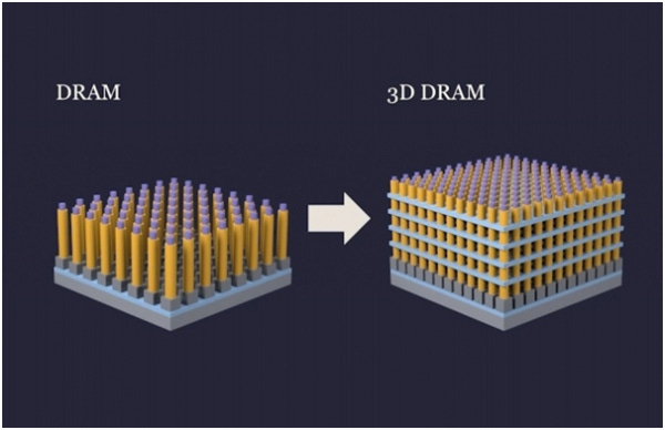
The industry is also beginning to explore 3D DRAM, in which memory cells are stacked vertically within a single chip. In conventional DRAM, cells sit side by side on a single flat layer of silicon, and capacity has been increased by shrinking the cells and packing them more closely together. This approach, however, is close to its physical limits. 3D DRAM instead builds upward, stacking several layers of cells in the same footprint, as shown in the photo below. (This is distinct from HBM, which bonds separate, fully fabricated DRAM dies on top of one another in a packaging step.)
A shift toward 3D DRAM could work modestly in China’s favor, because it would move more of the manufacturing difficulty away from photolithography and toward high-aspect-ratio etching and thin-film deposition (both covered in the equipment section below). Those are areas where China’s domestic equipment industry is still behind, but where it has made faster progress than in photolithography.
Semiconductor manufacturing equipment
The dominant cost of a new fab is equipment, which makes up about 70-80% of the total investment, with the physical building accounting for the rest. The full production process involves about 1,000 individual steps and takes more than four months from blank wafer to finished AI chip. Each step requires its own specialized tools produced by a handful of companies in the US, Japan, and the Netherlands. As described in this report, the key stages, repeated hundreds of times to build the chip layer by layer, work as follows:
Deposition coats the wafer with an ultra-thin layer of new material, either a metal for wiring or an insulator to keep layers separate.
Lithography then projects a circuit pattern onto a light-sensitive coating (photoresist) on that layer, using ultraviolet light through a mask (like a stencil). This step is central to shrinking the chip’s features—how small they can be printed—and uses the single most expensive piece of equipment in the fab, the photolithography scanner.
Etching carves away material wherever the pattern is exposed, cutting the intended circuit structures into the silicon.
Ion implantation injects specific atoms into targeted regions of the wafer to change their electrical properties—this is how transistors get their ability to switch on and off.
Chemical mechanical planarization (CMP) polishes the wafer surface perfectly flat after each layer is built, so subsequent steps, like deposition, etching, or patterning, can proceed cleanly; without it, tiny bumps from earlier layers would compound into defects.
Cleaning removes residues, particles, and chemical contaminants between steps, as contamination at the nanometer scale can ruin an entire chip.
Metrology and inspection tools measure dimensions, check alignment between layers, and scan for defects throughout the process. Early detection allows some defects to be repaired, or allows the manufacturer to discard defective wafers early on.
After all layers have been built, the wafer enters testing, and each individual chip (“die”) on the wafer is probed to identify which ones work. The wafer is then diced into individual chips, and the working dies move to packaging, where they are mounted in protective housings with electrical connections. For many AI chips, advanced packaging is an additional critical step, with technologies like TSMC’s CoWoS placing the processor die alongside HBM stacks on a shared silicon interposer, enabling the fast data transfer that AI workloads require.
Photolithography
Photolithography, the most complex and important type of SME, is where China is furthest behind. EUV photolithography, essentially necessary for chips at 5nm and below, is the most complex piece of equipment in the semiconductor supply chain. Lithography machines alone account for roughly 20% of a new fab’s total capital investment. A modern chip contains tens of billions of transistors, spread across many precisely aligned layers. Although even at the most advanced nodes, fabs use DUV for the bulk of layers, the most critical, smallest-feature layers require EUV. Without EUV for those critical layers, a foundry must substitute DUV multipatterning (printing the same layer in multiple passes), which is slower, more error-prone, and thus more expensive. For the most advanced nodes, as well as future ones, DUV multipatterning may not be able to replace EUV at all.
Shanghai Micro Electronics Equipment (SMEE) is China’s oldest photolithography maker, but has reached only a 4% market share, and this only in i-line tools, a technology used for MEMS, sensors, and power electronics rather than advanced-node fabrication. The global lithography market is a near-monopoly, with ASML (Netherlands) holding over 85% of DUV immersion shipments and being the sole supplier of EUV systems. Nikon (Japan) still produces immersion DUV scanners capable of supporting advanced-node multipatterning, though these are older argon fluoride systems, produced at marginal scale. Canon (Japan) has stepped back from DUV photolithography to pursue nanoimprint lithography, a different paradigm that has seen little adoption, alongside i-line steppers for legacy nodes. Together, Nikon and Canon account for only about 6% of the lithography equipment market. Neither company makes EUV machines.
Photolithography machines are extraordinarily complex, perhaps the most complex machines ever built. An EUV machine, for instance, needs a powerful light source and mirrors polished to near-atomic perfection. Every part must be made and assembled with extreme precision, and must operate with extreme precision and control. The entire system has to run in a vacuum, because otherwise its short-wavelength light would be absorbed by air. A single EUV machine contains around 100,000 parts, and shipping it requires 40 freight containers, 3 cargo planes, and 20 trucks.
Export controls have cut China off from advanced lithography
Since 2019, ASML has been blocked from exporting its EUV systems to China after the US pressured the Dutch government. In 2023 and 2024, Dutch export controls were expanded to cover most advanced DUV systems, with both the Netherlands and Japan introducing parallel controls on these systems. China’s companies stockpiled wafer fabrication equipment in 2024, before the restrictions took effect, accounting for some 40% of global sales. ASML’s older 1980i immersion DUV shipments to China jumped from 14 units in 2021 to 89 in 2024, while sales of the more advanced 2050i and 2100i, both hit by Dutch controls in 2023-2024, collapsed to zero. By 2024, 70% of ASML’s global immersion DUV shipments went to China. Despite export controls, ASML’s revenue from China increased from about 15% in 2021 to about 33% in 2025. This spending surge has partly been interpreted as pre-emptive stockpiling of DUV systems in anticipation of further tightening.
DUV lithography
DUV machines come in two types, dry and immersion. In an immersion system, the gap between the lens and the silicon wafer is filled with a liquid, typically purified water, instead of air. Water has a higher refractive index than air, which shortens the light’s effective wavelength as it crosses that gap, and a shorter effective wavelength lets the machine print finer features than a dry system does. Immersion DUV machines are relevant for AI chipmaking in a few ways:
Direct fabrication of older nodes. With multipatterning, immersion DUV can produce chips at 7nm (2018), and potentially 5nm (2020).
Non-critical layers for advanced-node processes. Even in the most advanced-node processes, only a subset of layers require EUV. The remaining layers are still patterned with immersion DUV, so scaling production below 5nm still requires many immersion DUV machines.
HBM production. HBM2E and earlier generations are made entirely with DUV. Even the newer HBM3E and HBM4 DRAM dies use EUV only for a handful of the most critical layers; the bulk of advanced DRAM production still relies heavily on immersion DUV.
DUV multipatterning cannot fully substitute for EUV
Beyond EUV research, what matters practically is what China can produce with its existing DUV tools. For mature nodes at 45nm and above, where dry DUV suffices, China is well supplied by a mix of domestic and imported systems—SMIC, Hua Hong, and Nexchip collectively run millions of wafer starts per month at these nodes. For 28nm and below, Chinese fabs rely on imported immersion DUV tools from ASML, a stockpile of machines bought before Dutch and Japanese export controls tightened in 2023, 2024, and 2025, as well as some less advanced immersion DUV tools that remain unrestricted.
As described in the section on chip fabrication, 7nm chips can be made without EUV using immersion DUV multipatterning; TSMC’s first 7nm process used this approach before later versions introduced EUV. SMIC has used the same basic workaround for Huawei’s Kirin chips. But this approach comes with steep trade-offs in cost, yield, and throughput, as each additional pass must align at the nanometer scale. ASML’s most advanced DUV immersion scanners (the Twinscan NXT series) can achieve overlay accuracy of around 2.5nm and throughput of 200 to 300 wafers per hour.
China holds a substantial installed base of ASML DUV scanners, including immersion systems capable of supporting 7nm production. But while the approach works, the volume is limited, and the economics are poor. The yields are roughly one-third of TSMC’s, and costs per wafer are approximately 50% higher.
Another long-term concern is that these machines age. Imported DUV tools require maintenance every six months from ASML itself; without this maintenance, the existing Chinese fleet would likely degrade significantly within a year. Spare parts, software updates, and servicing for the banned immersion DUV systems are also restricted. China’s domestic alternatives are still catching up: SMEE is working toward an immersion DUV system suitable for 28nm process node production, and Yuliangsheng supplied its first 28nm system to SMIC in 2025 for early testing, reportedly experimenting with multipatterning to produce 7nm chips. Domestic tools capable of supporting sub-10nm production (even with multipatterning) are, however, not expected before 2030.
EUV lithography
It took ASML about two decades to go from serious development of EUV to its first commercial shipment. The difficulty is spread across several uniquely complex subsystems, each made by only one or two suppliers in the world:
Light source. Tin droplets are fired into a vacuum chamber 50,000 times per second. A high-power CO2 laser hits each droplet twice, vaporizing it into a plasma 40 times hotter than the Sun’s surface, which emits EUV light. The drive laser is supplied exclusively by Trumpf (Germany), while the full light source is assembled by Cymer in San Diego, California, which ASML acquired in 2013.
Collector mirror. A large curved mirror channels EUV photons from the plasma into the optical system. Only Zeiss (Germany) can build it.
Multi-layer mirrors. The scanner contains 10-14 mirrors polished to near-atomic smoothness. Each reflects only about 70% of EUV light, so only about 2% of the source’s output reaches the wafer. Zeiss (Germany) is again the sole producer.
Photomasks. The specialized low-defect substrates that carry the circuit pattern. HOYA and AGC (both from Japan) produce them and together hold about 93% of the global EUV photomask market.
Pellicle. A thin protective film shields the photomask during printing. Mitsui Chemicals (Japan) manufactures them commercially under a license from ASML.
That is why even serious Chinese progress in prototype systems should be interpreted cautiously. Building something that emits EUV light is not the same as building something that can support high-volume, commercially competitive chip production.
SiCarrier, a Shenzhen state-backed semiconductor equipment maker with close ties to Huawei, has emerged as the key coordinator linking domestic photolithography efforts and extending into EUV-adjacent optics through its stake in Zetop Technologies.
The absence of publicly verified data for Chinese tools makes tracking progress difficult. With that caveat, here’s what we can piece together. The table below maps all entities active in China’s EUV and advanced DUV ecosystem—equipment makers, coordinators, state research institutes, universities, and defense-industrial groups—alongside their specific subsystem focus and current maturity.
China’s EUV prototypes are still far from production tools
Reuters reported in December 2025 that China had constructed a prototype EUV photolithography machine inside a high-security facility in Shenzhen, under the oversight of China’s Central Science and Technology Commission, a top Party-level body created in 2023 to centralize national strategy over science and technology. The prototype was reportedly completed in early 2025 and is undergoing testing. It can generate EUV light but has not yet produced functional chips. The prototype would still need dramatic improvements in source power, conversion efficiency, mirror reflectivity, uptime, and precision optics before approaching commercial viability, as the gap between generating EUV light and actual chip production is substantial. The machine is described as physically much larger than ASML’s commercial systems, filling nearly an entire factory floor.
The project was built partly using components from older, pre-controls-era ASML machines acquired through secondary markets. Former ASML engineers, recruited with signing bonuses of $420,000 to $700,000 plus housing subsidies, played a significant role. The program has been described as analogous to the Manhattan Project: a top-down national effort, designated as one of Xi Jinping’s top strategic priorities, that mobilizes thousands of engineers across state research institutes and private firms under Huawei’s coordination. Work is reportedly conducted in secured facilities under strict secrecy, with some recruits issued identification cards under false names, instructed to use aliases, and teams deliberately isolated from one another.
China’s lack of EUV lithography severely constrains its chip manufacturing
Several key EUV components are produced by only a single supplier, exclusively for ASML. Only Trumpf (Germany) makes the CO2 drive laser. Only Zeiss (Germany) makes the multi-layer mirrors and optics (and since 2016, ASML has owned a 25% stake in Zeiss’s Semiconductor Manufacturing Technology subsidiary). Cymer, which assembles the full EUV light source, has been a wholly-owned ASML subsidiary since 2013. Berliner Glas, a specialty optics supplier, was acquired by ASML in 2020. Because these components have no economic alternative, Chinese firms could not procure them through normal commercial channels even in the absence of export controls. (In fact, our understanding is that ASML’s suppliers’ suppliers are also contractually prevented from selling parts to other companies.) And because no ASML EUV machines have ever shipped to China, Chinese researchers have no deployed system to study directly.
China’s progress is uneven across these subsystems, but it lags far behind on all of them. For the multi-layer mirrors that bounce EUV light through the scanner, ASML uses 10-14 molybdenum-silicon mirrors polished to near-atomic smoothness, each reflecting about 70% of EUV light. Only Zeiss SMT (Germany) can produce them at production grade. Chinese researchers at the Changchun Institute of Optics, Fine Mechanics and Physics (CIOMP), a Chinese Academy of Sciences institute, have achieved a reflectivity of about 65% using domestic Mo/Si mirrors. The commercial arm, Zetop Technologies, part-owned by SiCarrier and CIOMP, is working to scale these mirrors for lithography. Even this five-point reflectivity gap compounds across 10-14 sequential mirror bounces, meaning a Chinese system at 65% delivers only 35-50% as much EUV light to the wafer as ASML’s.
This has forced Chinese researchers toward entirely different light sources, perhaps developed in parallel with a laser-produced plasma (LPP) light source similar to that used by ASML:
Tsinghua University is developing a steady-state microbunching (SSMB) system that would use a 100-150-meter-circumference particle accelerator (roughly the size of two basketball courts) to generate continuous EUV light, targeting a power output above 1,000 W, higher than ASML’s about 600 W. Rather than shrink the lithography machine for export as ASML does, the proposed design co-locates multiple lithography machines around one central accelerator in a single large facility, effectively a chipmaking campus built around one light source. Construction of a dedicated SSMB-EUV facility in Xiong’an began in early 2025.
Harbin Institute of Technology is pursuing a laser-discharge plasma (LDP) source, which uses a solid-state laser combined with high-voltage electrode discharge to vaporize tin droplets and reportedly reaches around 100 W. LDP scales poorly to the powers needed for advanced-node lithography and is more commonly used for photomask defect inspection, so this path may end up as a supporting technology rather than a direct replacement for ASML’s light source. Both approaches are scientifically novel but unproven at high-volume manufacturing scale.
Most industry analysts do not expect a Chinese DUV immersion tool capable of supporting 7nm production via multipatterning before 2030, and even then, the resulting tools would likely lag ASML’s in yield and cost. Faster indigenization later this decade is possible—SMEE has announced systems capable of 28nm production, and SiCarrier tools are reportedly being tested by SMIC—but a first-generation domestic immersion tool would almost certainly be a long way from competitive. For EUV, Beijing’s stated target for a prototype capable of producing functional chip patterns is 2028, while 2030 is the more widely cited realistic expectation among outside analysts. A commercially viable EUV system is likely a decade or more away.
Even achieving a working prototype would not mean commercial readiness. ASML shipped its first EUV prototype in 2006 but did not make its first commercial shipment (the NXE:3400B) until 2017, 11 years later, and EUV-made chips did not appear in consumer products until 2019 with Samsung’s Galaxy Note 10. China may compress that timeline somewhat by hiring former ASML employees, buying older ASML components on the secondary market, and studying ASML’s own development pathway. Reverse engineering is more feasible for DUV than for EUV, as Chinese fabs operate many ASML DUV machines they can disassemble and study, whereas no EUV machine has ever been delivered to China. Still, turning a working prototype into commercially viable chip production could take years or decades.
Reports of China’s EUV prototypes and other hardware advancements must be interpreted with caution. China’s centrally directed industrial policy creates strong incentives for local governments, universities, and firms to exaggerate progress. Announcing breakthroughs serves as currency for recognition and funding within Beijing’s competitive industrial ecosystem, and there is little vetting of these claims. The most notorious example is HSMC, a Wuhan-backed company that burned through more than $2 billion without producing a single chip. The same system also fragments the supply chain. Provincial and municipal governments compete to nurture their own fully self-contained semiconductor clusters rather than coordinate around a single national effort, resulting in duplicated projects, small fabs, and spread-out capital. The prototypes may well constitute real scientific achievements, but even if so, they are many years away from being capable of volume production.
While China is making measurable progress on DUV and early-stage EUV machines, ASML is developing High-NA EUV machines, capable of printing features roughly 1.7 times smaller than standard EUV with less multipatterning. Intel has installed the first High-NA EUV tool, while TSMC appears to be postponing adoption due to its high cost.
Etch, clean, deposition, metrology, and more
China’s SME self-sufficiency remains limited overall. The share of domestically manufactured equipment installed in Chinese fabs reached roughly 35% in 2025, surpassing the government’s 30% target. But this aggregate figure is most likely skewed by mature and legacy-node tools (at 28nm and above), where domestic substitution is easier, rather than reflecting fully indigenous advanced-node production. The equivalent share for advanced-node equipment (7nm and below) is almost certainly much lower, but no reliable public breakdown exists.
Beijing is now pushing for 70% by 2027. Even so, China’s total equipment spending remained near record levels at $49 billion in 2025. Analysis of global market share data from 2019 to 2024 shows that Chinese companies are making real inroads in several equipment categories, even as the most advanced segments remain out of reach. Whether the 70% target is achievable depends heavily on the type of equipment. Whereas domestic substitution in etching and deposition already exceeds 40%, photolithography, the most critical and expensive step, remains around 18% overall, a figure that reflects tools for older process nodes and packaging rather than the DUV tools relevant for advanced semiconductor manufacturing. For advanced front-end production, China still has no competitive domestic immersion DUV tool shipping at scale.
Deposition tools coat wafers with ultra-thin layers of material—metal for wiring, insulators to electrically separate chip features, or barrier films to prevent contamination. China’s position varies dramatically across the three main types:
In physical vapor deposition (PVD), which vaporizes solid material to coat the wafer, Naura has grown from 1% to roughly 10% of the global market between 2019 and 2024. Applied Materials (US) still leads with roughly 86%, though it is losing 2-4 percentage points per year to Chinese competitors. Naura’s gains are primarily at mature nodes; for advanced-node processes, Applied Materials remains dominant.
In chemical vapor deposition (CVD), which uses chemical reactions to build up thin films, Chinese firms rose from 1% to 7% of the global market between 2019 and 2024, led by Piotech and Naura. The US still holds 78%. At YMTC (Yangtze Memory Technologies, China’s largest NAND flash maker), Piotech now supplies nearly a third of the installed CVD equipment, up from 15%, displacing foreign tools.
In atomic layer deposition (ALD), the most advanced and precise category, which deposits films one atom layer at a time and is essential for leading-edge nodes, China holds less than 1% of the global market as of 2024. ASM International (Netherlands), Tokyo Electron (Japan), Kokusai (Japan), and Lam Research (US) together control about 88% of the segment, making ALD the widest gap in China’s equipment portfolio.
Etching tools carve circuit patterns into the wafer after lithography. Dry etching, which uses reactive gas plasmas rather than liquid chemicals to remove material and is relied on more heavily than wet etching at advanced nodes for its greater precision, is where Chinese firms have made real progress. The global dry etch market remains dominated by US firms Lam Research and Applied Materials (together holding roughly 60%) and Japan’s Tokyo Electron (about 15%). Chinese companies Naura and AMEC together hold roughly 11% of the market, up from under 3% in 2019, though these sales are largely equipment for older process nodes.
On the specific capability of high-aspect-ratio etching, which is critical for 3D memory and HBM stacking, AMEC produces a tool capable of etching features with a 60:1 aspect ratio (a hole sixty times deeper than it is wide), a notable achievement but roughly 6-8 years behind the global frontier. Its tool is comparable to what non-Chinese manufacturers offered around 2018 and 2019 and cannot support HBM production beyond HBM2E. A successor promising 90:1 aspect ratios is under development and would narrow the gap to 2-3 years, but its market entry now looks closer to 2027 than the 2025 timeline AMEC originally signaled. For comparison, Lam Research’s latest cryogenic etch tools—a technique not yet available in Chinese equipment—are designed to reach ratios above 100:1. AMEC is investing heavily to close this gap, with R&D spending up 54% year-on-year in the first half of 2025, but it still spends roughly a fifth of what Lam Research allocates to R&D.
Cleaning tools remove residues, particles, and chemical contaminants between fabrication steps; contamination at the nanometer scale can ruin an entire chip, so cleaning accounts for a large share of the process steps. The global cleaning market is moderately concentrated. SCREEN Semiconductor Solutions (Japan), Tokyo Electron (Japan), Lam Research and Applied Materials (US), plus China’s ACM Research, together account for about 65% of revenue in 2024, with SCREEN retaining overall leadership. ACM is the only Chinese firm in the global top tier. Cleaning is also China’s strongest equipment sub-sector, with over 50% domestic self-sufficiency, driven by ACM and Naura. ACM tools are now deployed in HBM production at SK Hynix and Micron, and ACM is targeting HBM4-compatible systems by 2026.
CMP tools polish the wafer surface flat between layers. Chinese firms’ share of the global CMP market grew from roughly 3% to 11% between 2019 and 2024, driven almost entirely by Hwatsing Technology. Applied Materials (US) still leads at roughly 60% of the global market with more advanced capabilities. Hwatsing is also expanding into ion implantation through its acquisition of Xinyu Semiconductor, a strategically important move because ion implantation is one of China’s weakest equipment segments, with domestic self-sufficiency at just 1.4% and two US firms (Applied Materials and Axcelis) controlling over 80% of the global market.
Metrology and inspection tools measure feature dimensions, check layer-to-layer alignment, and scan for defects throughout fabrication—essential for yield at advanced nodes, where a defect of a few nanometers can ruin a chip. The segment is even more concentrated than testing. KLA (US) holds roughly 63% of the global metrology and inspection market as of 2024, up from about 50% in 2010, with Applied Materials a distant second at under 8%. KLA’s share in reticle (photomask) inspection exceeds 80%. In China, the domestic substitution rate for metrology tools reached roughly 25% in 2025 (up from about 15% in 2022), but this figure aggregates all process nodes and is almost certainly concentrated at mature nodes; no Chinese firm offers a competitive alternative for advanced-node inspection.
Semiconductor testing verifies that finished chips work correctly, and the complexity of the test depends on the chip’s complexity. In linear and discrete testing (the simplest category, used for basic components like transistors and diodes) Chinese firms Hangzhou Changchuan and AccoTEST have captured nearly 70% of the global market. China has also entered burn-in testing (which stress-tests chips at high temperatures to catch early failures; 9% global share) and SoC testing (which verifies complex integrated circuits, such as AI chips; 5% global share) since 2020. However, the most advanced SoC and memory test segments remain dominated by Advantest (Japan, about 58% global share) and Teradyne (US, about 23%).
Advanced packaging tools are increasingly important for AI chips, which rely on integrating multiple smaller chips (“chiplets”) into a single package. Two relevant variants of advanced packaging are 2.5D, where multiple chips are arranged on an “interposer” chip that facilitates communication, and 3D, where chips are stacked on top of each other. Such techniques include through-silicon vias (TSVs), Chip-on-Wafer-on-Substrate (CoWoS), and hybrid bonding. The advanced packaging process needs many different SME, including both wafer fabrication tools and assembly tools. The global market for the wafer fabrication tools used in advanced packaging is dominated by the US (65%), with Japan a distant second (15%), and China third (7%).
Chinese firms’ gains are concentrated in specific segments. They have gained about 10 percentage points in global share in etch and clean tools for advanced packaging since 2019, and in packaging deposition, they have surpassed Japan to become the second-largest supplier behind the US. Naura, for example, launched a TSV etcher for 12-inch wafers in 2020 and has since developed a plasma etching process that produces TSVs with 11.8-micron openings at 116-micron depth. But in higher-value advanced-packaging segments, especially hybrid bonding, China is likely at an early stage of development. Hybrid bonding is already used in current 3D stacking products such as AMD’s 3D V-Cache and in YMTC’s NAND architecture, and may become important for future HBM generations. Naura reportedly unveiled one of China’s first 12-inch die-to-wafer hybrid bonding systems in March 2026.
Across these categories, a handful of state-backed national champions are carving out positions in moderately complex equipment segments such as etching, cleaning, CVD, and CMP at mature nodes, and are expected to reinvest their revenue into R&D targeting harder segments like advanced-node ALD, ion implantation, and lithography, though Chinese firms still hold under 1% of the global ALD market and a near-zero share of lithography.
The four most important Chinese SME companies are Naura (etching, deposition, cleaning, and thermal processing), AMEC (etching and thin-film deposition), Piotech (CVD), and Hwatsing (CMP). Naura is the largest. Its 2025 revenue is forecast at about $7 billion (up from $4.2 billion in 2024), and it has climbed to sixth in the global ranking of SME suppliers by revenue in 2025—the only Chinese firm in the top tier, trailing only ASML, Applied Materials, Lam Research, Tokyo Electron, and KLA. Its order backlog runs through Q1 2027.
The Chinese state is investing heavily in its semiconductor industry. Big Fund III, the third phase of the National Integrated Circuit Industry Investment Fund, launched in May 2024 with $48 billion in capital, spending on materials, wafer-fabrication equipment, and chip companies across the supply chain rather than photolithography specifically. That headline figure is roughly on par with the €43 billion of funding in the EU Chips Act and the $39 billion in direct grants and loans in the US CHIPS Act, though the CHIPS Act also includes an estimated $46 billion in tax credits for chip manufacturing. Big Fund I ($19 billion, launched 2014) and Big Fund II ($29 billion, launched 2019) added another $48 billion in combined headline commitments, bringing the three phases’ total to about $95 billion.
On top of that, at least 15 local-government semiconductor funds add another $25 billion, with broader state subsidies (grants, tax incentives, low-interest loans, land concessions) estimated at around $50 billion more. These headline numbers come with caveats. The Big Fund disbursement has been marred by corruption investigations, with China’s Central Commission for Discipline Inspection launching a 2022 sweep of leading figures across the Big Fund and its management firms. Cases like Wuhan’s HSMC underscore that committed funding doesn’t always translate into effective semiconductor capability.
Veronika Blablová was funded through the Pivotal Research Fellowship during this work.
We’re grateful to the following people for providing thoughtful and constructive feedback on earlier drafts of this work: Raghav Akula, James Nicholas Bryant, Naci Cankaya, Jacob Feldgoise, Jack Freed, Hamish Low, Antoine Maier, Konstantin Pilz, Robi Rahman, Maxwell Roberts, Filip Šebok, and Kar Mun Nicole Wong. Their careful reading, questions, and suggestions substantially improved the final piece. Any remaining errors or shortcomings are entirely our own.
Throughout this text, “AI chip” refers to data center chips—the hardware used to train and run frontier AI models—rather than other AI chips, such as those found in phones, cameras, cars, and other devices.
Biren Technology draws on founding talent linked to SenseTime as well as NVIDIA, Qualcomm, and AMD; Enflame Technology and MetaX were founded by former AMD engineers; and Moore Threads was established by a former China executive of NVIDIA.
An “H100-equivalent” is a unit gained by dividing a given chip’s theoretical computational performance with the computational performance of an NVIDIA H100. Given that this conversion uses theoretical computational performance, and ignores memory bandwidth and other specifications, it’s most relevant to training workloads, which are typically compute-bound.
Under the BIS Advanced Computing rules (October 2022, updated October 2023), AI chips above a Total Processing Performance (TPP) of 4800 (or above 1600 combined with a Performance Density (PD) of 5.92) require a license for export to Chinese customers. In addition, Chinese chip designers that use US EDA software need a license to send chip-design files to foreign foundries, and foundries face a due-diligence red flag for chip designs exceeding 50 billion transistors and with HBM. See CSET for more on the October 2023 updates.
In May 2026, Huawei published a paper on what it calls the “Tau (τ) Scaling Law”, a proposed successor to Moore’s Law that measures progress in chips by minimizing the time constant τ (signal propagation delay) rather than by shrinking transistors. The aim is to continue raising performance and density through a “LogicFolding” architecture that distributes a chip’s internal circuits across vertically stacked wafer layers. Using this design, Huawei aims to “shorten wiring inside chips and considerably improve performance”. Huawei says Ascend chips are expected to fully adopt the approach by 2030. The fact that Huawei is pursuing this kind of architectural workaround is evidence that it is not capable of manufacturing cutting-edge AI chips.
This estimate is based on data compiled from reports on shipment quantities and per-chip technical specs. The 2025 shipment estimates draw on IDC via Reuters for Huawei (~812K Ascend 910Cs and 910Bs), Bloomberg for Cambricon (~150K Siyuan 590s, derived from the 2026 500K target framed as “more than triple 2025 output”), Reuters for Alibaba T-Head (~265K, most likely Zhenwus), IPO filings for Enflame (45,362 S60 chips produced January-September 2025, annualized to ~60K), KrAsia for Baidu Kunlunxin (~60K Kunlun P800), the Iluvatar CoreX HKEX prospectus (23.5K disclosed in Sep 2025, annualized to 30K), HelloChinaTech for MetaX (~25K), and partial-year industry filings for Biren (2,216 BR106 shipped in H1 2025, against 9,344 BR106 + 298 BR110 across full-year 2024; the prospectus notes that H2 2024 sales run higher than H1 2024 and that H1 2025 already exceeded H1 2024, so we extrapolate the full year to roughly 4,500-10,000 — from doubling H1 at the low end to repeating 2024’s level at the high end, we use ~10,000 for the visual) and a revenue-based estimate for Moore Threads, which discloses revenue, not unit shipments (The prospectus puts AI-compute products at 94.85% of H1 2025 revenue, all built on two data-center chips: S4000 and S5000. Full-year 2025 revenue was RMB 1.51B; at ~95% AI-compute, that’s ~RMB 1.43B. Dividing by an assumed per-GPU average selling price of RMB 50,000-100,000 implies ~14,000-30,000 chips. As it is reported as cluster systems, not standalone cards; the estimate likely overstates the chip count, so we use ~20K for the visual.). The per-chip performance data is from Epoch AI’s ML Hardware dataset, supplemented by reported specs or specs estimates for newer Chinese chips not yet in the dataset. The aggregate compute is calculated as Chips shipped × FP16 TFLOPS per chip, summed across designers, and expressed in H100-equivalents (each chip’s FP16 throughput ÷ the 989 TFLOPS of an NVIDIA H100). This makes for a total of about 770,000 H100-equivalents. Note that our tallies sum to about 1.4 million units, whereas Epoch AI reports 1.7 million units sold in 2025 by Chinese AI chip designers, so the real number might be somewhat higher.
OpenAI’s Stargate Abilene facility is planned to house “more than 450,000 NVIDIA GB200 GPUs”. These are likely 450,000 B200 GPUs. At about 2.5 H100-equivalents per B200 chip, the facility’s planned installed compute is about 1.1 million H100-equivalents. The comparison contrasts one year of Chinese chip shipments against a single US facility’s installed capacity, so it is not an apples-to-apples comparison.
As of end-2024, the largest state-affiliated shareholder is Datang Holdings (about 14%), a subsidiary of the state-owned China Information and Communication Technologies Group Corporation (CICT), which provides communication infrastructure to the People’s Liberation Army. The National Integrated Circuit Industry Investment Fund—China’s primary state-backed vehicle for financing semiconductor development, known as the “Big Fund”—holds roughly 8% through its subsidiary Xinxin (Hong Kong) Investment, with an additional 1.6% via Big Fund II. CICT itself directly holds roughly 1%.
The claim that five of Huawei’s 11 affiliated fabs are capable of 7nm-and-below processes originates from South Korean media outlets The Elec and Quasarzone, citing unnamed industry sources, and was subsequently reported in English by Digitimes and WCCFTech. Huawei has not confirmed the claim, and no independent teardown or facility audit has confirmed 7nm output from any of Huawei’s affiliated fabs apart from SMIC itself.
In 2015, Tsinghua Unigroup, a conglomerate majority-owned by Tsinghua University and backed by China’s state semiconductor fund, made a $23 billion bid for Micron, which would have been the largest-ever Chinese acquisition of a US company. The Committee on Foreign Investment in the United States (CFIUS), the US government’s foreign investment watchdog, made clear it would not approve the deal on national security grounds.
Until early 2025, CXMT’s most advanced production sat at the threshold of the 2022 US export rules, which originally prohibited the supplying or servicing of fab equipment for DRAM at nodes below 18nm half-pitch. CXMT reportedly told US authorities that it uses a 18.5nm process node (just outside the restricted threshold), allowing it to keep sourcing and servicing advanced foreign fab tools. At the same time, the company presented research on a more aggressive 18nm half-pitch DRAM built with gate-all-around transistors—signaling capability that runs ahead of what the fab manufactures at scale. In December 2024, BIS tightened the rules and closed this potential loophole. The controls no longer depend on the node label and target memory cell area and DRAM density instead.
The two principal bonding approaches used for HBM stacking are thermocompression bonding with non-conductive film (TC-NCF), which applies high temperature (about 300°C) and force to bond dies via solder micro-bumps, and mass reflow with mold underfill (MR-MUF), which bonds at lower temperature and lower force and provides substantially better thermal dissipation. MR-MUF is the superior process, delivering higher yield than TC-NCF and handling heat far more effectively as stack heights increase. Whereas SK Hynix uses MR-MUF, Samsung and Micron have been unable to replicate it due to both technical and patent barriers. CXMT’s HBM products are expected to rely on TC-NCF bonding. However, a reported partnership between CXMT and YMTC could change this trajectory. YMTC’s Xtacking architecture—a wafer-to-wafer hybrid bonding process used in mass production of 3D NAND—is relevant because the HBM industry may migrate toward hybrid bonding for future generations. CXMT brings the DRAM process; YMTC brings the stacking technique.
 | A guest post by
|